l Ultra Low RDS(on) per Footprint Area l Low Thermal Resistance
l P-Channel MOSFET l One-third Footprint of SOT-23 l Sup...
l Ultra Low RDS(on) per Footprint Area l Low Thermal Resistance
l P-Channel
MOSFET l One-third Footprint of SOT-23 l Super Low Profile (<.8mm) l Available Tested on Tape & Reel
VDSS
-20V
PD - 93930F
IRF6100
HEXFET® Power
MOSFET
RDS(on) max
0.065Ω@VGS = -4.5V
0.095Ω@VGS = -2.5V
ID
-5.1A
-4.1A
Description
True chip-scale packaging is available from International Rectifier. Through the use of advanced processing techniques, and a unique packaging concept, extremely low on-resistance and the highest power densities in the industry have been made available for battery and load management applications. These benefits, combined with the ruggedized device design , that International Rectifier is well known for, provides the designer with an extremely efficient and reliable device.
G
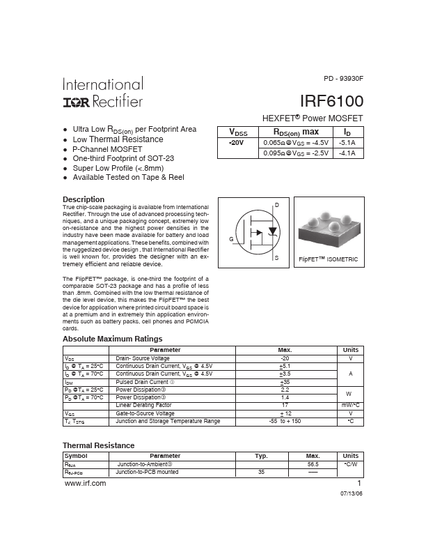
The FlipFET™ package, is one-third the footprint of a comparable SOT-23 package and has a profile of less than .8mm. Combined with the low thermal resistance of the die level device, this makes the FlipFET™ the best device for application where printed circuit board space is at a premium and in extremely thin application environments such as battery packs, cell phones and PCMCIA cards.
Absolute Maximum Ratings
VDS ID @ TA = 25°C ID @ TA = 70°C IDM PD @TA = 25°C PD @TA = 70°C
VGS TJ, TSTG
Parameter Drain- Source
Voltage
Continuous Drain Current, VGS @ 4.5V Continuous Drain Current, VGS @ 4.5V Pulsed Drain Current Power Dissipation Power Dissipation Linear Derating Factor
Gate-to-Source Volta...