www.DataSheet4U.com
IPB085N06L G
IPP085N06L G
OptiMOS® Power-Transistor
Features • For fast switching converters and ...
www.DataSheet4U.com
IPB085N06L G
IPP085N06L G
OptiMOS® Power-Transistor
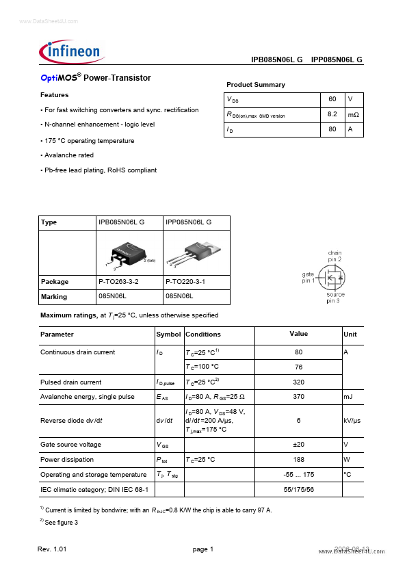
Features For fast switching converters and sync. rectification N-channel enhancement - logic level 175 °C operating temperature Avalanche rated Pb-free lead plating, RoHS compliant
Product Summary V DS R DS(on),max ID
SMD version
60 8.2 80
V mΩ A
Type
IPB085N06L G
IPP085N06L G
Type IPB085N06L G Package IPP085N06L G Marking
Package P-TO263-3-2 P-TO263-3-2 085N06L P-TO220-3-1
Marking P-TO220-3-1 085N06L 085N06L 085N06L
Maximum ratings, at T j=25 °C, unless otherwise specified Parameter Continuous drain current Symbol Conditions ID T C=25 °C1) T C=100 °C Pulsed drain current Avalanche energy, single pulse Reverse diode dv /dt Gate source
voltage Power dissipation Operating and storage temperature IEC climatic category; DIN IEC 68-1
1) 2)
Value 80 76 320 370 6 ±20
Unit A
I D,pulse E AS dv /dt V GS P tot T j, T stg
T C=25 °C2) I D=80 A, R GS=25 Ω I D=80 A, V DS=48 V, di /dt =200 A/µs, T j,max=175 °C
mJ kV/µs V W °C
T C=25 °C
188 -55 ... 175 55/175/56
Current is limited by bondwire; with an R thJC=0.8 K/W the chip is able to carry 97 A. See figure 3
Rev. 1.01
page 1
2006-06-13
www.DataSheet4U.com
IPB085N06L G
Parameter Symbol Conditions min. Thermal characteristics Thermal resistance, junction - case SMD version, device on PCB R thJC R thJA minimal footprint 6 cm2 cooling area3) Electrical characteristics, at T j=25 °C, unless otherwise specified Static characteristics Drain-...