IPB240N03S4L-R8
OptiMOS™-T2 Power-Transistor
Features • N-channel - Enhancement mode • AEC qualified • MSL1 up to 260°C...
IPB240N03S4L-R8
OptiMOS™-T2 Power-Transistor
Features N-channel - Enhancement mode AEC qualified MSL1 up to 260°C peak reflow 175°C operating temperature Green package (RoHS compliant) Ultra low Rds(on) 100% Avalanche tested
Product Summary V DS R DS(on) ID
30 V 0.76 mW 240 A
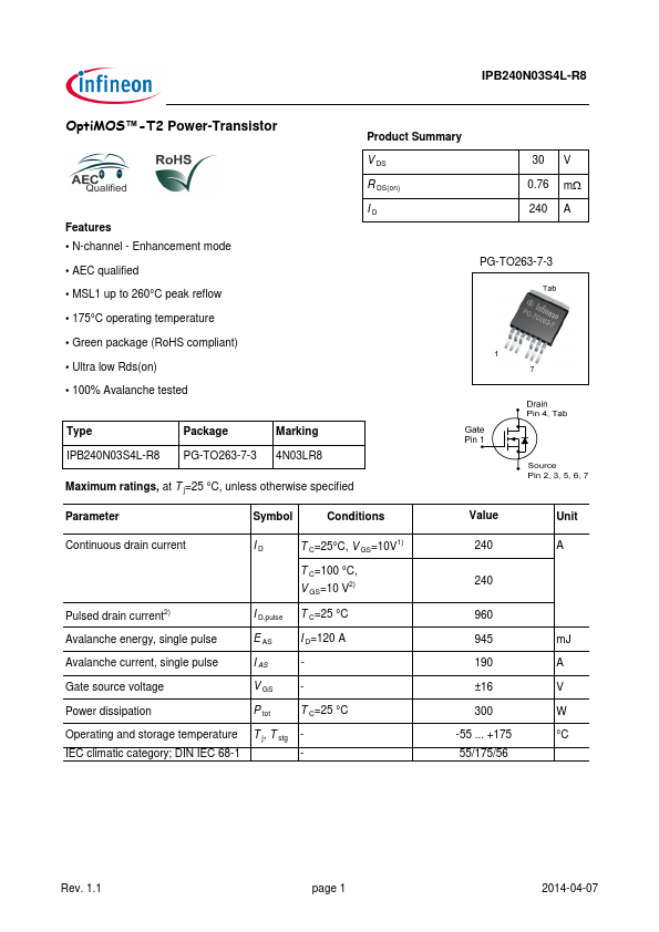
PG-TO263-7-3
Type IPB240N03S4L-R8
Package PG-TO263-7-3
Marking 4N03LR8
Maximum ratings, at T j=25 °C, unless otherwise specified
Parameter
Symbol
Conditions
Continuous drain current
I D T C=25°C, V GS=10V1)
T C=100 °C, V GS=10 V2)
Pulsed drain current2)
I D,pulse T C=25 °C
Avalanche energy, single pulse
E AS I D=120 A
Avalanche current, single pulse
I AS -
Gate source
voltage
V GS
-
Power dissipation
P tot T C=25 °C
Operating and storage temperature T j, T stg -
IEC climatic category; DIN IEC 68-1
-
Value
240
240
960 945 190 ±16 300 -55 ... +175 55/175/56
Unit A
mJ A V W °C
Rev. 1.1
page 1
2014-04-07
IPB240N03S4L-R8
Parameter
Symbol
Conditions
Thermal characteristics2)
Thermal resistance, junction - case SMD version, device on PCB
R thJC R thJA
minimal footprint 6 cm2 cooling area3)
min.
Values typ.
Unit max.
- - 0.5 K/W - - 62 - - 40
Electrical characteristics, at T j=25 °C, unless otherwise specified
Static characteristics Drain-source breakdown
voltage Gate threshold
voltage Zero gate
voltage drain current
Gate-source leakage current Drain-source on-state resistance Drain-source on-state resistance
V (BR)DSS V GS=0 V, I D= 1 mA
V GS(th) I ...