Type
IPP015N04N G IPB015N04N G
OptiMOS™3 Power-Transistor
Features • Fast switching MOSFET for SMPS • Optimized techno...
Type
IPP015N04N G IPB015N04N G
OptiMOS™3 Power-Transistor
Features Fast switching
MOSFET for SMPS Optimized technology for DC/DC converters Qualified according to JEDEC for target applications N-channel, normal level Excellent gate charge x R DS(on) product (FOM) Very low on-resistance R DS(on) 100% Avalanche tested Pb-free plating; RoHS compliant Halogen-free according to IEC61249-2-21 Type IPB015N04N G IPP015N04N G
1)
Product Summary V DS R DS(on),max ID 40 1.5 120 V mΩ A
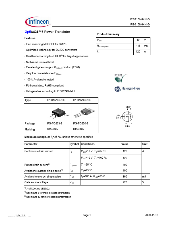
Package Marking
PG-TO263-3 015N04N
PG-TO220-3 015N04N
Maximum ratings, at T j=25 °C, unless otherwise specified Parameter Continuous drain current Symbol Conditions ID V GS=10 V, T C=25 °C V GS=10 V, T C=100 °C Pulsed drain current2) Avalanche current, single pulse 3) Avalanche energy, single pulse Gate source
voltage
1) 2) 3)
Value 120 120 400 100 865 ±20
Unit A
I D,pulse I AS E AS V GS
T C=25 °C T C=25 °C I D=100 A, R GS=25 Ω
mJ V
J-STD20 and JESD22 See figure 3 for more detailed information See figure 13 for more detailed information
www.DataSheet4U.net
Rev. 2.2
page 1
2009-11-16
IPP015N04N G IPB015N04N G
Maximum ratings, at T j=25 °C, unless otherwise specified Parameter Power dissipation Operating and storage temperature IEC climatic category; DIN IEC 68-1 Symbol Conditions P tot T j, T stg T C=25 °C Value 250 -55 ... 175 55/175/56 Unit W °C
Parameter
Symbol Conditions min.
Values typ. max.
Unit
Thermal characteristics Thermal resistance, junction - case SMD ve...