TECHNICAL DATA
IN74HCT132A
Quad 2-Input NAND Gate with Schmitt-Trigger Inputs
High-Performance Silicon-Gate CMOS
The I...
TECHNICAL DATA
IN74HCT132A
Quad 2-Input NAND Gate with Schmitt-Trigger Inputs
High-Performance Silicon-Gate
CMOS
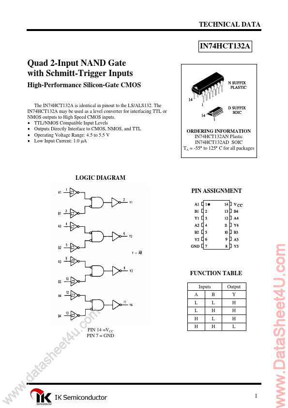
The IN74HCT132A is identical in pinout to the LS/ALS132. The IN74HCT132A may be used as a level converter for interfacing TTL or NMOS outputs to High Speed
CMOS inputs. TTL/NMOS Compatible Input Levels Outputs Directly Interface to
CMOS, NMOS, and TTL Operating
Voltage Range: 4.5 to 5.5 V Low Input Current: 1.0 µA
ORDERING INFORMATION IN74HCT132AN Plastic IN74HCT132AD SOIC TA = -55° to 125° C for all packages
LOGIC DIAGRAM PIN ASSIGNMENT
FUNCTION TABLE
Inputs A L L H H B L H L H Output Y H H H L
w
w
w
.d
e e h s a t a
. u t4
m o c
PIN 14 =VCC PIN 7 = GND
1
www.DataSheet4U.com
IN74HCT132A
MAXIMUM RATINGS*
Symbol VCC VIN VOUT IIN IOUT ICC PD Tstg TL
*
Parameter DC Supply
Voltage (Referenced to GND) DC Input
Voltage (Referenced to GND) DC Output
Voltage (Referenced to GND) DC Input Current, per Pin DC Output Current, per Pin DC Supply Current, VCC and GND Pins Power Dissipation in Still Air, Plastic DIP+ SOIC Package+ Storage Temperature Lead Temperature, 1 mm from Case for 10 Seconds (Plastic DIP or SOIC Package)
Value -0.5 to +7.0 -1.5 to VCC +1.5 -0.5 to VCC +0.5 ±20 ±25 ±50 750 500 -65 to +150 260
Unit V V V mA mA mA mW °C °C
Maximum Ratings are those values beyond which damage to the device may occur. Functional operation should be restricted to the Recommended Operating Conditions. +Derating - Plastic DIP: - 10 mW/°C from 65° to 125°...