TECHNICAL DATA
IN74HC574A
Octal 3-State Noninverting D Flip-Flop
High-Performance Silicon-Gate CMOS
N SUFFIX PLASTIC D...
TECHNICAL DATA
IN74HC574A
Octal 3-State Noninverting D Flip-Flop
High-Performance Silicon-Gate
CMOS
N SUFFIX PLASTIC DIP
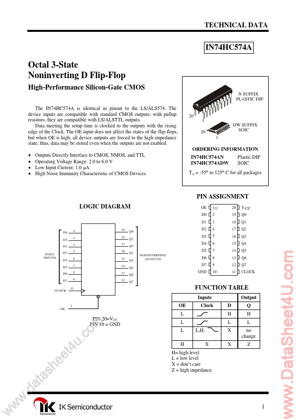
The IN74HC574A is identical in pinout to the LS/ALS574. The device inputs are compatible with standard
CMOS outputs; with pullup resistors, they are compatible with LS/ALSTTL outputs. Data meeting the setup time is clocked to the outputs with the rising edge of the Clock. The OE input does not affect the states of the flip-flops, but when OE is high, all device outputs are forced to the high-impedance state; thus, data may be stored even when the outputs are not enabled. Outputs Directly Interface to
CMOS, NMOS, and TTL Operating
Voltage Range: 2.0 to 6.0 V Low Input Current: 1.0 µA High Noise Immunity Characteristic of
CMOS Devices
20 1 20 1 DW SUFFIX SOIC
ORDERING INFORMATION IN74HC574AN IN74HC574ADW Plastic DIP SOIC
TA = -55° to 125° C for all packages
PIN ASSIGNMENT LOGIC DIAGRAM
OE D0 D1
D0 D1 D2 DATA INPUTS D3 D4 D5 D6 D7 CLOCK 2 3 4 5 6 7 8 9 11 19 18 17 16 15 14 13 12 Q0 Q1 Q2 Q3 Q4 Q5 Q6 Q7 NONINVERTING OUTPUTS
1 2 3 4 5 6 7 8 9 10
20 19 18 17 16 15 14 13 12 11
V CC Q0 Q1 Q2 Q3 Q4 Q5 Q6 Q7 CLOCK
D2 D3 D4 D5 D6 D7 GND
FUNCTION TABLE
Inputs Output D H L L,H, X X X Q H L no change Z OE L PIN 20=VCC PIN 10 = GND Clock
1 OE
w
w
w
.d
a t a
e h s
4 t e
c . u
om
L L H
H= high level L = low level X = don’t care Z = high impedance
1
www.DataSheet4U.com
IN74HC574A
MAXIMUM RATINGS*
Symbol VCC VIN VOUT IIN IOUT ICC PD Tstg TL...