TECHNICAL DATA
IN74ACT74
Dual D Flip-Flop with Set and Reset
High-Speed Silicon-Gate CMOS
The IN74ACT74 is identical i...
TECHNICAL DATA
IN74ACT74
Dual D Flip-Flop with Set and Reset
High-Speed Silicon-Gate
CMOS
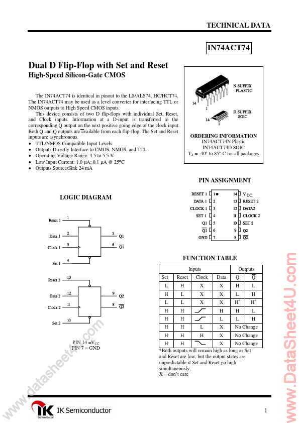
The IN74ACT74 is identical in pinout to the LS/ALS74, HC/HCT74. The IN74ACT74 may be used as a level converter for interfacing TTL or NMOS outputs to High Speed
CMOS inputs. This device consists of two D flip-flops with individual Set, Reset, and Clock inputs. Information at a D-input is transferred to the corresponding Q output on the next positive going edge of the clock input. Both Q and Q outputs are available from each flip-flop. The Set and Reset inputs are asynchronous. TTL/NMOS Compatible Input Levels Outputs Directly Interface to
CMOS, NMOS, and TTL Operating
Voltage Range: 4.5 to 5.5 V Low Input Current: 1.0 µA; 0.1 µA @ 25°C Outputs Source/Sink 24 mA
ORDERING INFORMATION IN74ACT74N Plastic IN74ACT74D SOIC TA = -40° to 85° C for all packages
PIN ASSIGNMENT LOGIC DIAGRAM
FUNCTION TABLE
Inputs Set L H L H H Reset H L L H H H H L H Clock X X X Data X X X H L X X Outputs Q H L H
*
Q L H H* L H
H L
w
w
w
.d
e e h s a t a
. u t4
PIN 14 =VCC PIN 7 = GND
m o c
H H
No Change No Change
H H X No Change *Both outputs will remain high as long as Set and Reset are low, but the output states are unpredictable if Set and Reset go high simultaneously. X = don’t care
1
www.DataSheet4U.com
IN74ACT74
MAXIMUM RATINGS*
Symbol VCC VIN VOUT IIN IOUT ICC PD Tstg TL
*
Parameter DC Supply
Voltage (Referenced to GND) DC Input
Voltage (Referenced to GND) DC Output
Voltage (...