TECHNICAL DATA
IN74ACT34
Hex Noninverter Buffer
High-Speed Silicon-Gate CMOS
The IN74ACT34 is identical in pinout to t...
TECHNICAL DATA
IN74ACT34
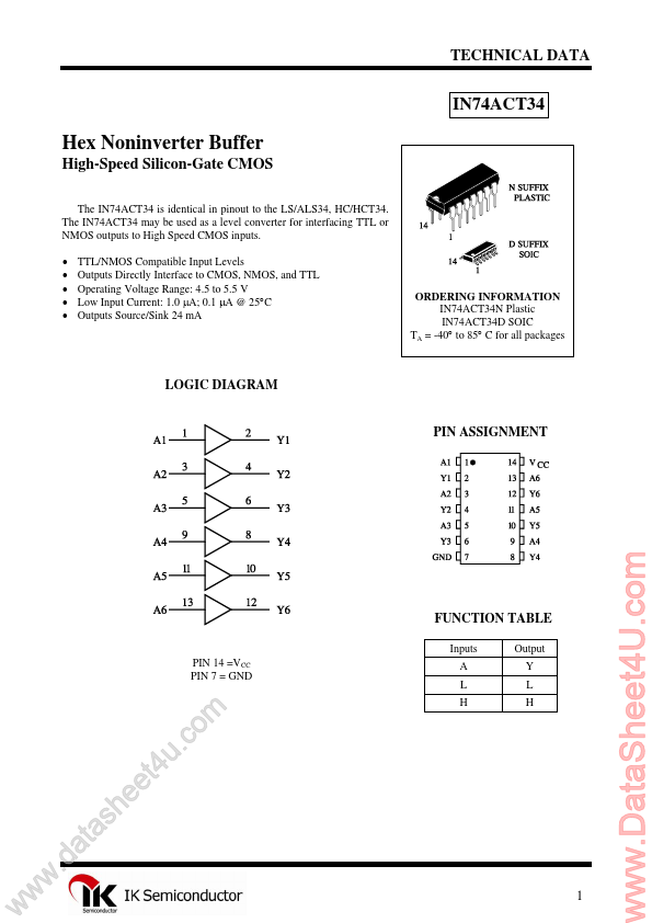
Hex Noninverter Buffer
High-Speed Silicon-Gate
CMOS
The IN74ACT34 is identical in pinout to the LS/ALS34, HC/HCT34. The IN74ACT34 may be used as a level converter for interfacing TTL or NMOS outputs to High Speed
CMOS inputs. TTL/NMOS Compatible Input Levels Outputs Directly Interface to
CMOS, NMOS, and TTL Operating
Voltage Range: 4.5 to 5.5 V Low Input Current: 1.0 µA; 0.1 µA @ 25°C Outputs Source/Sink 24 mA
ORDERING INFORMATION IN74ACT34N Plastic IN74ACT34D SOIC TA = -40° to 85° C for all packages
LOGIC DIAGRAM
PIN ASSIGNMENT
FUNCTION TABLE
Inputs PIN 14 =VCC PIN 7 = GND A L H Output Y L H
w
w
w
.d
e e h s a t a
. u t4
m o c
1
www.DataSheet4U.com
IN74ACT34
MAXIMUM RATINGS*
Symbol VCC VIN VOUT IIN IOUT ICC PD Tstg TL
*
Parameter DC Supply
Voltage (Referenced to GND) DC Input
Voltage (Referenced to GND) DC Output
Voltage (Referenced to GND) DC Input Current, per Pin DC Output Sink/Source Current, per Pin DC Supply Current, VCC and GND Pins Power Dissipation in Still Air, Plastic DIP+ SOIC Package+ Storage Temperature Lead Temperature, 1 mm from Case for 10 Seconds (Plastic DIP or SOIC Package)
Value -0.5 to +7.0 -0.5 to VCC +0.5 -0.5 to VCC +0.5 ±20 ±50 ±50 750 500 -65 to +150 260
Unit V V V mA mA mA mW °C °C
Maximum Ratings are those values beyond which damage to the device may occur. Functional operation should be restricted to the Recommended Operating Conditions. +Derating - Plastic DIP: - 10 mW/°C from 65° to 125°C...