8-Bit Bidirectional Universal Shift Register with Parallel I/O High-Speed Silicon-Gate CMOS
TECHNICAL DATA
IN74AC299
8-Bit Bidirectional Universal Shift Register with Parallel I/O
High-Speed Silicon-Gate CMOS
T...
TECHNICAL DATA
IN74AC299
8-Bit Bidirectional Universal Shift Register with Parallel I/O
High-Speed Silicon-Gate
CMOS
The IN74AC299 is identical in pinout to the LS/ALS299, HC/HCT299. The device inputs are compatible with standard
CMOS outputs; with pullup resistors, they are compatible with LS/ALS outputs. The IN74AC299 features a multiplexed parallel input/output data port to achieve full 8-bit handling in a 20 pin package. Due to the large output drive capability and the 3-state feature, this device is ideally suited for interface with bus lines in a bus-oriented system. Two Mode-Select inputs and two Output Enable inputs are used to choose the mode of operation as listed in the Function Table. Synchronous parallel loading is accomplished by taking both ModeSelect lines, S1 and S2, high. This places the outputs in the highimpedance state, which permits data applied to the data port to be clocked into the register. Reading out of the register can be accomplished when the outputs are enabled. The active-low asynchronous Reset overrides all other inputs. Outputs Directly Interface to
CMOS, NMOS, and TTL Operating
Voltage Range: 2.0 to 6.0 V Low Input Current: 1.0 µA; 0.1 µA @ 25°C High Noise Immunity Characteristic of
CMOS Devices Outputs Source/Sink 24 mA
ORDERING INFORMATION IN74AC299N Plastic IN74AC299DW SOIC TA = -40° to 85° C for all packages
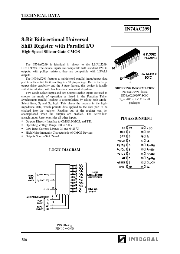
PIN ASSIGNMENT
LOGIC DIAGRAM
PIN 20=VCC PIN 10 = GND
386
IN74AC299
MAXIMUM RATINGS*
Symbol VCC VIN VOUT IIN IOUT...