TECHNICAL DATA
Hex Schmitt-Trigger Inverter
High-Speed Silicon-Gate CMOS
The IN74AC14 is identical in pinout to the LS/...
TECHNICAL DATA
Hex Schmitt-Trigger Inverter
High-Speed Silicon-Gate
CMOS
The IN74AC14 is identical in pinout to the LS/ALS14, HC/HCT14. The device inputs are compatible with standard
CMOS outputs; with pullup resistors, they are compatible with LS/ALS outputs. The IN74AC14 is useful to “square up” slow input rise and fall times. Due to the hysteresis
voltage of the Schmitt trigger, the IN74AC14 finds applications in noisy environments. Outputs Directly Interface to
CMOS, NMOS, and TTL Operating
Voltage Range: 2.0 to 6.0 V Low Input Current: 1.0 µA; 0.1 µA @ 25°C High Noise Immunity Characteristic of
CMOS Devices Outputs Source/Sink 24 mA
IN74AC14
ORDERING INFORMATION IN74AC14N Plastic IN74AC14D SOIC TA = -40° to 85° C for all packages
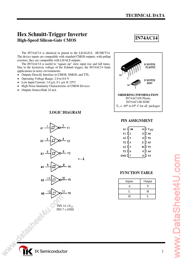
LOGIC DIAGRAM PIN ASSIGNMENT
FUNCTION TABLE
Inputs A L H Output Y H L
w
w
w
.d
e e h s a t a
. u t4
m o c
PIN 14 =VCC PIN 7 = GND
1
www.DataSheet4U.com
IN74AC14
MAXIMUM RATINGS*
Symbol VCC VIN VOUT IIN IOUT ICC PD Tstg TL
*
Parameter DC Supply
Voltage (Referenced to GND) DC Input
Voltage (Referenced to GND) DC Output
Voltage (Referenced to GND) DC Input Current, per Pin DC Output Sink/Source Current, per Pin DC Supply Current, VCC and GND Pins Power Dissipation in Still Air, Plastic DIP+ SOIC Package+ Storage Temperature Lead Temperature, 1 mm from Case for 10 Seconds (Plastic DIP or SOIC Package)
Value -0.5 to +7.0 -0.5 to VCC +0.5 -0.5 to VCC +0.5 ±20 ±50 ±50 750 500 -65 to +150 260
Unit V V V mA mA mA mW °C °C
M...