3.3V PHASE-LOCK LOOP CLOCK DRIVER
www.DataSheet4U.com
IDTCSP2510D 3.3V PHASE-LOCK LOOP CLOCK DRIVER
0°C TO 85°C TEMPERATURE RANGE
3.3V PHASE-LOCK LOOP ...
Description
www.DataSheet4U.com
IDTCSP2510D 3.3V PHASE-LOCK LOOP CLOCK DRIVER
0°C TO 85°C TEMPERATURE RANGE
3.3V PHASE-LOCK LOOP CLOCK DRIVER ZERO DELAY BUFFER
FEATURES: DESCRIPTION:
Phase-Lock Loop Clock Distribution for Synchronous DRAM Applications Distributes one clock input to one bank of ten outputs Output enable bank control External feedback (FBIN) pin is used to synchronize the outputs to the clock input signal No external RC network required for PLL loop stability Operates at 3.3V VDD tpd Phase Error at 166MHz: < ±150ps Jitter (peak-to-peak) at 166MHz: < ±75ps @ 166MHz Spread Spectrum Compatible Operating frequency 50MHz to 175MHz Available in 24-Pin TSSOP package
IDTCSP2510D
APPLICATIONS:
SDRAM Modules PC Motherboards Workstations
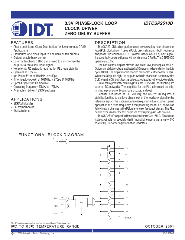
The CSP2510D is a high performance, low-skew, low-jitter, phase-lock loop (PLL) clock driver. It uses a PLL to precisely align, in both frequency and phase, the feedback (FBOUT) output to the clock (CLK) input signal. It is specifically designed for use with synchronous DRAMs. The CSP2510D operates at 3.3V. One bank of ten outputs provide low-skew, low-jitter copies of CLK. Output signal duty cycles are adjusted to 50 percent, independent of the duty cycle at CLK. The outputs can be enabled or disabled via the control G input. When the G input is high, the outputs switch in phase and frequency with CLK; when the G input is low, the outputs are disabled to the logic-low state. Unlike many products containing PLLs, the...
Similar Datasheet