2.5V TO 3.3V HIGH PERFORMANCE CLOCK BUFFER
IDT5V2305 2.5V TO 3.3V HIGH PERFORMANCE CLOCK BUFFER
2.5V TO 3.3V HIGH PERFORMANCE CLOCK BUFFER
INDUSTRIALTEMPERATURERA...
Description
IDT5V2305 2.5V TO 3.3V HIGH PERFORMANCE CLOCK BUFFER
2.5V TO 3.3V HIGH PERFORMANCE CLOCK BUFFER
INDUSTRIALTEMPERATURERANGE
IDT5V2305
FEATURES:
High performance 1:5 clock driver for general purpose applications
Operates up to 170MHz at VDD = 2.5V Operates up to 200MHz at VDD = 3.3V Pin-to-pin skew < 75ps at 3.3V operation VDD range: 2.3V to 3.6V Output enable glitch suppression Available in TSSOP and VFQFPN packages
DESCRIPTION:
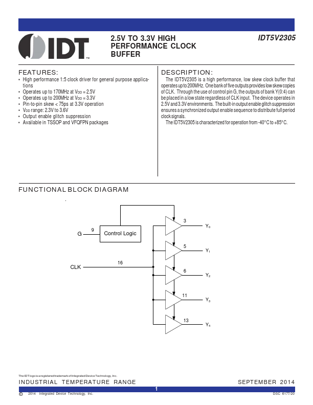
The IDT5V2305 is a high performance, low skew clock buffer that operates up to 200MHz. One bank of five outputs provides low skew copies of CLK. Through the use of control pin G, the outputs of bank Y(0:4) can be placed in a low state regardless of CLK input. The device operates in 2.5V and 3.3V environments. The built-in output enable glitch suppression ensures a synchronized output enable sequence to distribute full period clock signals.
The IDT5V2305 is characterized for operation from -40°C to +85°C.
FUNCTIONAL BLOCK DIAGRAM
9
G Control Logic
CLK
16
3 Y0
5 Y1
6 Y2
11 Y3
13 Y4
The IDT logo is a registered trademark of Integrated Device Technology, Inc.
INDUSTRIAL TEMPERATURE RANGE
c 2014 Integrated Device Technology, Inc.
1
SEPTEMBER 2014
DSC 6177/20
IDT5V2305 2.5V TO 3.3V HIGH PERFORMANCE CLOCK BUFFER
PIN CONFIGURATION
GND VDD Y0 GND
Y1 Y2 VDD GND
1 2 3 4 5 6 7 8
16 CLK 15 VDD 14 VDD 13 Y4 12 GND 11 Y3 10 VDD
9G
TSSOP TOP VIEW
INDUSTRIALTEMPERATURERANGE
CLK
VDD
1 16
VDD
2
15 VDD
Y0 3
14 NC
NC
4
GND
13
Y4
...
Similar Datasheet