FAST CMOS BUFFER/CLOCK DRIVER
Integrated Device Technology, Inc.
IDT54/74FCT810BT/CT
FEATURES:
• • • • • • • • 0.5 MIC...
FAST
CMOS BUFFER/CLOCK DRIVER
Integrated Device Technology, Inc.
IDT54/74FCT810BT/CT
FEATURES:
0.5 MICRON
CMOS technology Guaranteed low skew < 600ps (max.) Very low duty cycle distortion < 700ps (max.) Low
CMOS power levels TTL compatible inputs and outputs TTL level output
voltage swings High drive: –32mA IOH, 48mA IOL Two independent output banks with 3-state control – One 1:5 Inverting bank – One 1:5 Non-Inverting bank ESD > 2000V per MIL-STD-883, Method 3015; > 200V using machine model (C = 200pF, R = 0) Available in DIP, SOIC, SSOP, QSOP, CERPACK and
LCC packages Military product compliant to MIL-STD-883, Class B
DESCRIPTION:
The IDT54/74FCT810BT/CT is a dual bank inverting/ noninverting clock driver built using advanced dual metal
CMOS technology. It consists of two banks of drivers, one inverting and one non-inverting. Each bank drives five output buffers from a standard TTL-compatible input. The IDT54/ 74FCT810BT/CT have low output skew, pulse skew and package skew. Inputs are designed with hysteresis circuitry for improved noise immunity. The outputs are designed with TTL output levels and controlled edge rates to reduce signal noise. The part has multiple grounds, minimizing the effects of ground inductance.
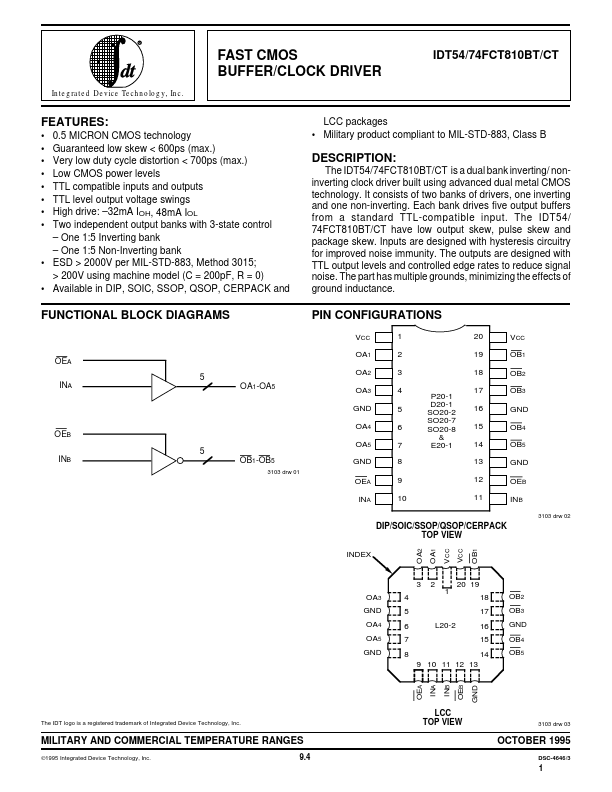
FUNCTIONAL BLOCK DIAGRAMS
PIN CONFIGURATIONS
VCC 1 2 3 4 5 6 7 8 9 10 P20-1 D20-1 SO20-2 SO20-7 SO20-8 & E20-1 20 19 18 17 16 15 14 13 12 11 VCC OB1 OB2 OB3 GND OB4 OB5 GND OEB INB
3103 drw 02
OEA 5 INA OA1-OA5
OA1 OA2 OA3 GND
OEB...