General Purpose Frequency Timing Generator
ICS951601
Preliminary Product Preview
General Purpose Frequency Timing Generator
Recommended Application: General Purp...
Description
ICS951601
Preliminary Product Preview
General Purpose Frequency Timing Generator
Recommended Application: General Purpose Clock Generator
Output Features: 17 - PCI clocks selectable,
either 33.33MHz or 66.6MHz @ 3.3V 1 - 48MHz @ 3.3V 1 - REF @ 3.3V, 14.318MHz.
Features: Programable Spread spectrum precentage for EMI
control Uses external 14.318MHz crystal Select pins for frequency select
Key Specifications: PCI – PCI output skew within same bank @
33MHz: <170ps
PCI – PCI output skew within same bank@ 66MHz: <340ps
Cycle to Cycle Jitter PCI @ 33MHz: <200ps
Cycle to Cycle Jitter PCI @ 66MHz: <200ps Cycle to Cycle Jitter 48MHz: <350ps
Cycle to Cycle Jitter REF: <500ps
Slew Rate: 1.5 - 4 V/ns. (PCI spec.)
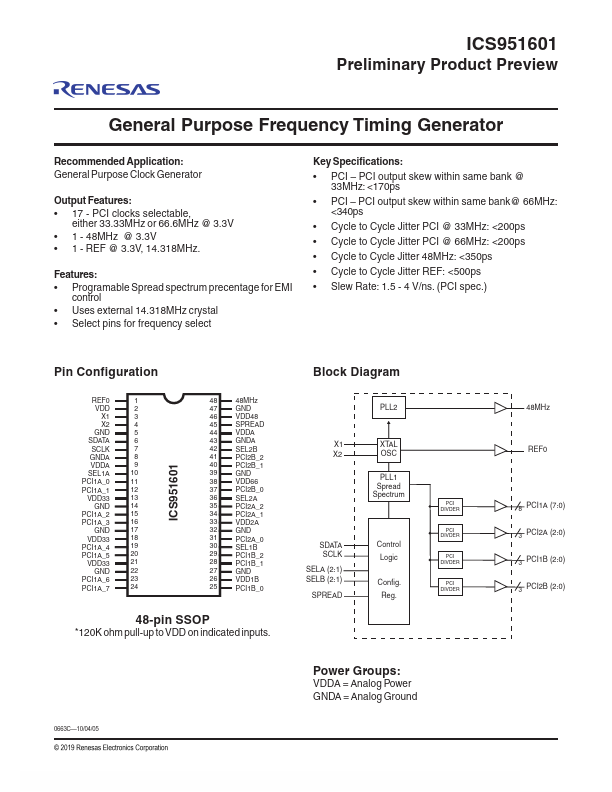
Pin Configuration
REF0
1
VDD
2
X1
3
X2
4
GND
5
SDATA
6
SCLK
7
GNDA
8
VDDA
9
SEL1A
10
PCI1A_0
11
PCI1A_1
12
VDD33
13
GND
14
PCI1A_2
15
PCI1A_3
16
GND
17
VDD33
18
PCI1A_4
19
PCI1A_5
20
VDD33
21
GND
22
PCI1A_6
23
PCI1A_7
24
ICS951601
48
48MHz
47
GND
46
VDD48
45
SPREAD
44
VDDA
43
GNDA
42
SEL2B
41
PCI2B_2
40
PCI2B_1
39
GND
38
VDD66
37
PCI2B_0
36
SEL2A
35
PCI2A_2
34
PCI2A_1
33
VDD2A
32
GND
31
PCI2A_0
30
SEL1B
29
PCI1B_2
28
PCI1B_1
27
GND
26
VDD1B
25
PCI1B_0
48-pin SSOP
*120K ohm pull-up to VDD on indicated inputs.
0663C—10/04/05
Block Diagram
PLL2
X1
XTAL
X2
OSC
PLL1 Spread Spectrum
SDATA SCLK
SELA (2:1) SELB (2:1)
SPREAD
Control Logic
Config. Reg.
...
Similar Datasheet