www.DataSheet4U.com
Integrated Circuit Systems, Inc.
ICS87931I
LOW SKEW, 1-TO-6 LVCMOS/LVTTL CLOCK MULTIPLIER/ZERO DEL...
www.DataSheet4U.com
Integrated Circuit Systems, Inc.
ICS87931I
LOW SKEW, 1-TO-6 LV
CMOS/LVTTL CLOCK MULTIPLIER/ZERO DELAY BUFFER
FEATURES
Fully integrated PLL 6 LV
CMOS/LVTTL outputs, 7Ω typical output impedance Selectable differential CLK0, nCLK0 or LV
CMOS/LVTTL clock for redundant clock applications Maximum output frequency: 150MHz VCO range: 220MHz to 480MHz External feedback for “zero delay” clock regeneration Output skew, Same Frequency: 300ps (maximum) Output skew, Different Frequency: 400ps (maximum) Cycle-to-cycle jitter: 100ps (maximum) 3.3V supply
voltage -40°C to 85°C ambient operating temperature Pin compatible with MPC931
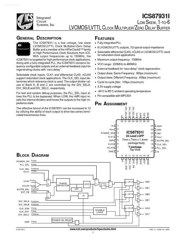
GENERAL DESCRIPTION
The ICS87931I is a low
voltage, low skew LV
CMOS/LVTTL Clock Multiplier/Zero Delay HiPerClockS™ Buffer and a member of the HiPerClockS™ family of High Performance Clock Solutions from ICS. With output frequencies up to 150MHz, the ICS87931I is targeted for high performance clock applications. Along with a fully integrated PLL, the ICS87931I contains frequency configurable outputs and an external feedback input for regenerating clocks with “zero delay”.
,&6
Selectable clock inputs, CLK1 and differential CLK0, nCLK0 support redundant clock applications. The CLK_SEL input determines which reference clock is used. The output divider values of Bank A, B and C are controlled by the DIV_SELA, DIV_SELB and DIV_SELC, respectively. For test and system debug purposes, the PLL_SEL input allows the PLL to be bypas...