ICS8305I
LOW SKEW, 1-TO-4, MULTIPLEXED DIFFERENTIAL/ LVCMOS-TO-LVCMOS/LVTTL FANOUT BUFFER
GENERAL DESCRIPTION
The ICS83...
ICS8305I
LOW SKEW, 1-TO-4, MULTIPLEXED DIFFERENTIAL/ LV
CMOS-TO-LV
CMOS/LVTTL FANOUT BUFFER
GENERAL DESCRIPTION
The ICS8305I is a low skew, 1-to-4, Differential/LV
CMOS-toLV
CMOS/LVTTL Fanout Buffer. The ICS8305I has selectable clock inputs that accept either differential or single ended input levels. The clock enable is internally synchronized to eliminate runt pulses on the outputs during asynchronous assertion/deassertion of the clock enable pin. Outputs are forced LOW when the clock is disabled. A separate output enable pin controls whether the outputs are in the active or high impedance state.
Guaranteed output and part-to-part skew characteristics make the ICS8305I ideal for those applications demanding well defined performance and repeatability.
FEATURES
4 LV
CMOS/LVTTL outputs Selectable differential or LV
CMOS/LVTTL clock inputs CLK, nCLK pair can accept the following differential
input levels: LVPECL, LVDS, LVHSTL, HCSL, SSTL LV
CMOS_CLK supports the following input types:
LV
CMOS, LVTTL Maximum output frequency: 350MHz Output skew: 40ps (maximum) Part-to-part skew: 700ps (maximum) Additive phase jitter, RMS: 0.04ps (typical) 3.3V core, 3.3V, 2.5V or 1.8V output operating supply -40°C to 85°C ambient operating temperature Lead-Free package fully RoHS compliant
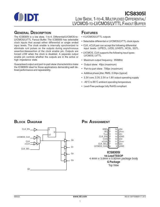
BLOCK DIAGRAM
CLK_EN
LV
CMOS_CLK CLK
nCLK
CLK_SEL
00 11
D Q
LE
OE
PIN ASSIGNMENT
GND 1 16 Q0
OE 2
1 5 VDDO
VDD 3
14 Q1
CLK_EN 4 13 GND
CLK 5 12 Q2
Q0
nCLK 6
1 1 VDDO
CLK_SEL 7 1...