Integrated Circuit Systems, Inc.
ICS83052I
2:1, SINGLE-ENDED MULTIPLEXER
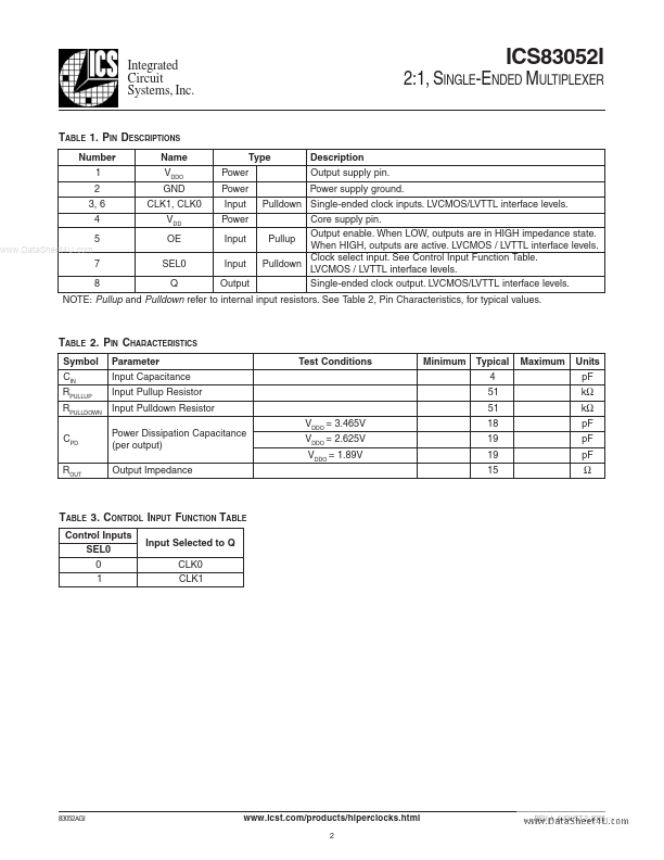
TABLE 1. PIN DESCRIPTIONS
Number 1 2 3, 6 4 5...
Integrated Circuit Systems, Inc.
ICS83052I
2:1, SINGLE-ENDED MULTIPLEXER
TABLE 1. PIN DESCRIPTIONS
Number 1 2 3, 6 4 5
www.DataSheet4U.com
Name VDDO GND CLK1, CLK0 VDD OE SEL0 Q Power Power Input Power Input Input
Type
Description Output supply pin. Power supply ground.
Pulldown Single-ended clock inputs. LV
CMOS/LVTTL interface levels. Core supply pin. Output enable. When LOW, outputs are in HIGH impedance state. Pullup When HIGH, outputs are active. LV
CMOS / LVTTL interface levels. Clock select input. See Control Input Function Table. Pulldown LV
CMOS / LVTTL interface levels. Single-ended clock output. LV
CMOS/LVTTL interface levels.
7 8
Output
NOTE: Pullup and Pulldown refer to internal input resistors. See Table 2, Pin Characteristics, for typical values.
TABLE 2. PIN CHARACTERISTICS
Symbol CIN RPULLUP RPULLDOWN CPD ROUT Parameter Input Capacitance Input Pullup Resistor Input Pulldown Resistor Power Dissipation Capacitance (per output) Output Impedance VDDO = 3.465V VDDO = 2.625V VDDO = 1.89V Test Conditions Minimum Typical 4 51 51 18 19 19 15 Maximum Units pF kΩ kΩ pF pF pF Ω
TABLE 3. CONTROL INPUT FUNCTION TABLE
Control Inputs SEL0 0 1 Input Selected to Q CLK0 CLK1
83052AGI
www.icst.com/products/hiperclocks.html
2
REV. A AUGUST 2, 2005
Integrated Circuit Systems, Inc.
ICS83052I
2:1, SINGLE-ENDED MULTIPLEXER
ABSOLUTE MAXIMUM RATINGS
Supply
Voltage, VDD Inputs, VI Outputs, VO Package Thermal Impedance, θJA Storage Temperature, TSTG
www.DataSheet4U.com
4.6V...