www.DataSheet4U.com
ICS552-02
LOW SKEW 2 INPUT MUX AND 1 TO 8 CLOCK BUFFER
Description
The ICS552-02 is a low skew, sin...
www.DataSheet4U.com
ICS552-02
LOW SKEW 2 INPUT MUX AND 1 TO 8 CLOCK BUFFER
Description
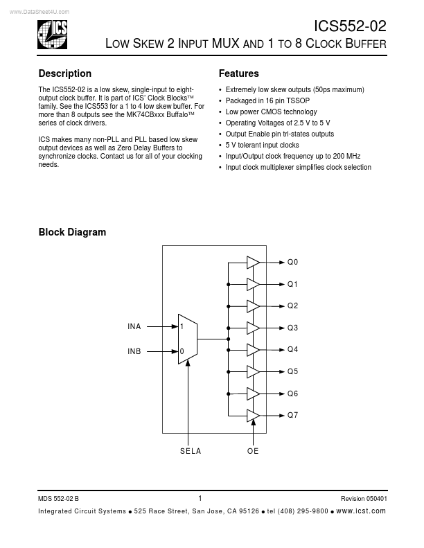
The ICS552-02 is a low skew, single-input to eightoutput clock buffer. It is part of ICS’ Clock BlocksTM family. See the ICS553 for a 1 to 4 low skew buffer. For more than 8 outputs see the MK74CBxxx BuffaloTM series of clock drivers. ICS makes many non-PLL and PLL based low skew output devices as well as Zero Delay Buffers to synchronize clocks. Contact us for all of your clocking needs.
Features
Extremely low skew outputs (50ps maximum) Packaged in 16 pin TSSOP Low power
CMOS technology Operating
Voltages of 2.5 V to 5 V Output Enable pin tri-states outputs 5 V tolerant input clocks Input/Output clock frequency up to 200 MHz Input clock multiplexer simplifies clock selection
Block Diagram
Q0 Q1 Q2 IN A 1 Q3 Q4 Q5 Q6 Q7
IN B
0
S E LA
OE
MDS 552-02 B In tegr ated C ir cu it S yst ems
q
1
5 25 Ra ce Str eet, San Jose, C A 95 126
q
Revision 050401 tel ( 408) 2 95-9 800
q
www. i c s t. c om
P R E L I M I N A RY I N FO R M ATI O N
ICS552-02 LOW SKEW 2 INPUT MUX AND 1 TO 8 CLOCK
Pin Assignment
OE VDD Q0 Q1 Q2 Q3 GND INB 1 2 3 4 5 6 7 8 16 15 14 13 12 11 10 9 SELA VDD Q7 Q6 Q5 Q4 GND INA
Input Source Select
SELA
0 1
Input
INB INA
16 Pin TSSOP
Pin Descriptions
Pin Number
1 2 3 4 5 6 7 8 9 10 11 12 13 14 15 16
Pin Name
OE VDD Q0 Q1 Q2 Q3 GND INB INA GND Q4 Q5 Q6 Q7 VDD SELA
Pin Type
Input Power Output Output Output Output Power Input Input Power Output Output Out...