(HY27UGxx Series) 2G-Bit NAND Flash
w
e e Document h Title S / 256Mx16bit) NAND Flash Memory 4Gbit (512Mx8bit a at .D History Revision w w
Revision No.
0.0...
Description
w
e e Document h Title S / 256Mx16bit) NAND Flash Memory 4Gbit (512Mx8bit a at .D History Revision w w
Revision No.
0.0
U 4 t
.
m o c
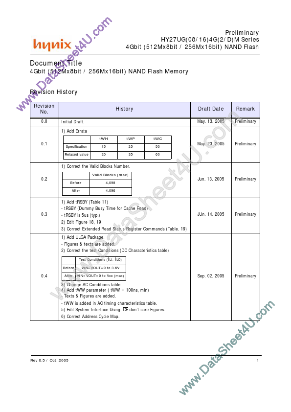
Preliminary HY27UG(08/16)4G(2/D)M Series 4Gbit (512Mx8bit / 256Mx16bit) NAND Flash
History
Draft Date
May. 13. 2005
Remark
Preliminary
Initial Draft. 1) Add Errata
tWH tWP 25 35 tWC 50 60
0.1
Specification Relaxed value
15 20
May. 23. 2005
1) Correct the Valid Blocks Number. 0.2
Valid Blocks (max) Before After 4,098 4,096
1) Add tRSBY (Table 11) - tRSBY (Dummy Busy Time for Cache Read) 0.3 - tRSBY is 5us (typ.) 2) Edit Figure 18, 19 1) Add ULGA Package.
3) Correct Extended Read Status Register Commands (Table. 19) - Figures & texts are added.
2) Correct the test Conditions (DC Characteristics table)
Test Conditions (ILI, ILO) Before VIN=VOUT=0 to 3.6V VIN=VOUT=0 to Vcc (max)
0.4
After
w
Rev 0.5 / Oct. 2005
3) Change AC Conditions table 4) Add tWW parameter ( tWW = 100ns, min) - Texts & Figures are added. - tWW is added in AC timing characteristics table. 5) Edit System Interface Using CE don’t care Figures.
w
w
.D
t a
S a
e h
t e
U 4
.c
m o
Preliminary
Jun. 13. 2005
Preliminary
JUn. 14. 2005
Preliminary
Sep. 02. 2005
Preliminary
6) Correct Address Cycle Map.
w
w
w
.D
at
h S a
t e e
4U
.
m o c
1
Preliminary HY27UG(08/16)4G(2/D)M Series 4Gbit (512Mx8bit / 256Mx16bit) NAND Flash Revision History
Revision No. History
7) Correct PKG dimension (TSOP PKG) CP Before After 0.050 0.100
-Continued-
Draf...
Similar Datasheet