www.datasheet4u.com
HD74LVC1G53
2–channel Analog Multiplexer/Demultiplexer
REJ03D0155–0300Z Rev.3.00 Jul. 02, 2004
Des...
www.datasheet4u.com
HD74LVC1G53
2–channel Analog Multiplexer/Demultiplexer
REJ03D0155–0300Z Rev.3.00 Jul. 02, 2004
Description
The HD74LVC1G53 has 2–channel analog multiplexer/demultiplexer in a 6-pin package. Applications include signal gating chopping, modulation or demodulation (modem), and signal multiplexing for analog to digital to analog conversion systems. Low
voltage and high-speed operation is suitable for the battery powered products (e.g., notebook computers), and the low power consumption extends the battery life.
Features
The basic gate function is lined up as renesas uni logic series. Supply
voltage range: 1.65 to 5.5 V Operating temperature range: –40 to +85°C Control input: VIH (Max.) = 5.5 V (@VCC = 0 V to 5.5 V) Ordering Information
Part Name HD74LVC1G53CPE HD74LVC1G53CLE Package Type WCSP-6 pin Package Code TBS-6V TBS-6AV CP CL Package Abbreviation Taping Abbreviation (Quantity) E (3,000 pcs/reel)
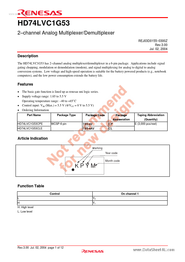
Article Indication
Marking Year code Month code
KPYM
Function Table
Control L H H: High level L: Low level Y0 Y1 On channel 1
Rev.3.00 Jul. 02, 2004 page 1 of 12
HD74LVC1G53
w w w . d a t a s h e e t 4 u . c o m
Pin Arrangement
0.9 mm Height 0.5 mm 0.5 mm pitch 0.17 mm 6–Ball (CP) 0.23 mm 6–Ball (CL)
Y0
3
4
COM
GND
2
5
VCC
1.4 mm
Pin#1 INDEX
Y1
1
6
A
(Bottom view)
(Top view)
Logic Diagram
Y1 A Y0
1 6 3 4
Rev.3.00 Jul. 02, 2004 page 2 of 12
HD74LVC1G53
www.datasheet4u.com
Absolute Maximum Ratings
Item Supply
voltage range Inp...