HD74LV374A
Octal Edge-Triggered D-type Flip-Flops with 3-state Outputs
ADE-205-275 (Z) 1st Edition April 1999 Descripti...
HD74LV374A
Octal Edge-Triggered D-type Flip-Flops with 3-state Outputs
ADE-205-275 (Z) 1st Edition April 1999 Description
The HD74LV374A has eight edge trigger D type flip flops with three state outputs in a 20 pin package. Data at the D inputs meeting set up requirements, are transferred to the Q outputs on positive going transitions of the clock input. When the clock input goes low, data at the D inputs will be retained at the outputs until clock input returns high again. When a high logic level is applied to the output control input, all outputs go to a high impedance state, regardless of what signals are present at the other inputs and the state of the storage elements. Low-
voltage and high-speed operation is suitable for the battery-powered products (e.g., notebook computers), and the low-power consumption extends the battery life.
Features
VCC = 2.0 V to 5.5 V operation All inputs VIH (Max.) = 5.5 V (@VCC = 0 V to 5.5 V) All outputs VO (Max.) = 5.5 V (@VCC = 0 V) Typical VOL ground bounce < 0.8 V (@VCC = 3.3 V, Ta = 25°C) Typical VOH undershoot > 2.3 V (@VCC = 3.3 V, Ta = 25°C) Output current ±8 mA (@VCC = 3.0 V to 3.6 V), ±16 mA (@VCC = 4.5 V to 5.5 V)
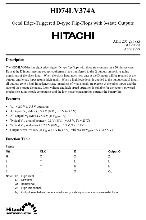
Function Table
Inputs OE H L L L Note: H: L: X: Z: Q0 : CLK X ↑ ↑ ↓ D X L H X Output Q Z L H Q0
High level Low level Immaterial High impedance Output level before the indicated steady state input conditions were established.
HD74LV374A
Pin Arrangement
OE 1 1Q 2 1D 3 2D 4 2Q 5 3Q 6 3D 7 4D 8 4Q 9 GND 10
...