HD74HC4024
7-stage Binary Counter
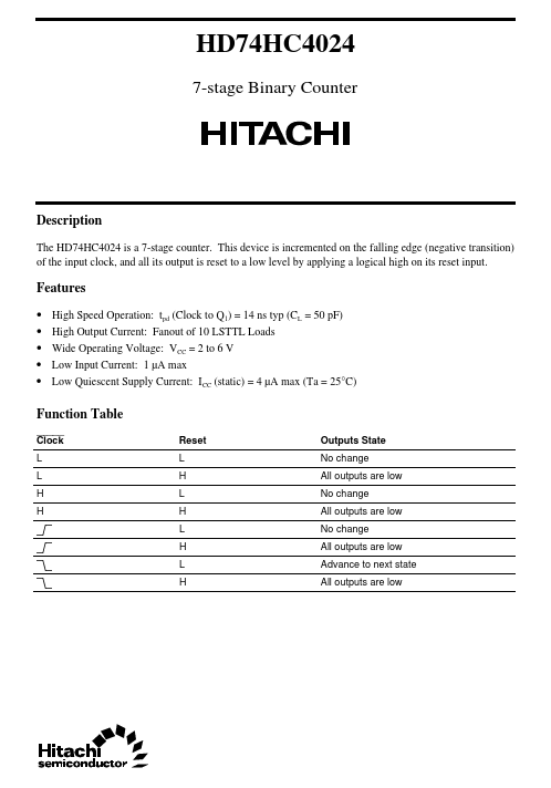
Description
The HD74HC4024 is a 7-stage counter. This device is incremented on the fa...
HD74HC4024
7-stage Binary Counter
Description
The HD74HC4024 is a 7-stage counter. This device is incremented on the falling edge (negative transition) of the input clock, and all its output is reset to a low level by applying a logical high on its reset input.
Features
High Speed Operation: tpd (Clock to Q1) = 14 ns typ (CL = 50 pF) High Output Current: Fanout of 10 LSTTL Loads Wide Operating
Voltage: VCC = 2 to 6 V Low Input Current: 1 µA max Low Quiescent Supply Current: ICC (static) = 4 µA max (Ta = 25°C)
Function Table
Clock L L H H Reset L H L H L H L H Outputs State No change All outputs are low No change All outputs are low No change All outputs are low Advance to next state All outputs are low
HD74HC4024
Pin Arrangement
Clock Reset Q7 Q6 Q5 Q4 GND
1 2 3 4 5 6 7 (Top view) R Q7 Q6 Q5 Q4 Q3 C
14 13 Q1 Q2 12 11 10 9 8
VCC NC Q1 Q2 NC Q3 NC
Block Diagram
Clock
C
Q
C
Q
C
Q
C
Q
R Reset
Q
R
Q
R
Q
R
Q
Q1
Q2
Q6
Q7
2
HD74HC4024
DC Characteristics
Ta = 25°C Item Input
voltage Symbol VIH Ta = –40 to +85°C Max — — — 0.5 1.35 1.8 — — — — — 0.1 0.1 0.1 0.33 0.33 ±1.0 40 µA µA I OL = 4 mA I OL = 5.2 mA Vin = VCC or GND Vin = VCC or GND, Iout = 0 µA V I OH = –4 mA I OH = –5.2 mA Vin = VIH or VIL I OL = 20 µA V Vin = VIH or VIL I OH = –20 µA V Unit V Test Conditions
VCC (V) Min Typ Max Min 2.0 4.5 6.0 1.5 — 3.15 — 4.2 — — — — — — — — — — 0.5 1.5 3.15 4.2 —
VIL
2.0 4.5 6.0
1.35 — 1.8 — 1.9 4.4 5.9 4.13 5.63 — — —
Output
voltage
VOH
2.0 4...