HD74AC368/HD74ACT368
Hex Inverter Buffer with 3-State Output
Features
• 3-State Outputs Drive Bus Lines or Buffer Memor...
HD74AC368/HD74ACT368
Hex Inverter Buffer with 3-State Output
Features
3-State Outputs Drive Bus Lines or Buffer Memory Address Registers Outputs Source/Sink 24 mA HD74ACT368 has TTL-Compatible Inputs
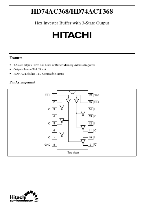
Pin Arrangement
OE1 I O I O I O GND
1 2 3 4 5 6 7 8 (Top view)
16 VCC 15 OE2 14 I 13 O 12 I 11 O 10 I 9 O
HD74AC368/HD74ACT368
Logic Symbol
OE
I
O
Pin Names
OE1, OE2 I O 3-State Output: Enable Input (Active Low) Inputs Outputs
Truth Table
Inputs OE L L H H L X Z : : : : High
Voltage Level Low
Voltage Level Immaterial High Impedance I L H X Output O L H Z
DC Characteristics (unless otherwise specified)
Item Maximum quiescent supply current Maximum quiescent supply current Maximum ICC/input (HD74ACT368) Symbol I CC I CC I CCT Max 80 8.0 1.5 Unit µA µA mA Condition VIN = VCC or ground, VCC = 5.5 V, Ta = Worst case VIN = VCC or ground, VCC = 5.5 V, Ta = 25°C VIN = VCC – 2.1 V, VCC = 5.5 V, Ta = Worst case
2
HD74AC368/HD74ACT368
AC Characteristics: HD74AC368
Ta = +25°C CL = 50 pF Item Propagation delay Symbol t PLH VCC (V)*1 3.3 5.0 Propagation delay t PHL 3.3 5.0 Enable time t PZH 3.3 5.0 Enable time t PZL 3.3 5.0 Disable time t PHZ 3.3 5.0 Disable time t PLZ 3.3 5.0 Note: 1.
Voltage Range 3.3 is 3.3 V ± 0.3 V
Voltage Range 5.0 is 5.0 V ± 0.5 V Min 1.0 1.0 1.0 1.0 1.0 1.0 1.0 1.0 1.0 1.0 1.0 1.0 Typ 7.0 5.0 7.0 4.5 9.0 7.0 10.0 7.5 9.5 7.5 9.0 7.0 Max 9.0 7.0 9.0 7.0 13.0 9.5 12.5 10.0 12.0 10.0 12.5 10.0 Ta = –40°C to +85°C CL = 50 pF Min 1.0 1.0 1.0 1.0 1.0 1.0 ...