8-bit Shift Register
HD74AC166/HD74ACT166
8-bit Shift Register
Description
The HD74AC166/HD74ACT166 is an 8-bit, serial or parallel-in, seri...
Description
HD74AC166/HD74ACT166
8-bit Shift Register
Description
The HD74AC166/HD74ACT166 is an 8-bit, serial or parallel-in, serial-out shift register using edge triggered D-type flip-flops. Serial and parallel entry are synchronous, with state changes initiated by the rising edge of the clock. An asynchronous Master Reset overrides other inputs and clears all flip-flops. The circuit can be clocked from two sources or one CP input can be used to trigger the other.
Features
Outputs Source/Sink 24 mA HD74ACT166 has TTL-Compatible Inputs
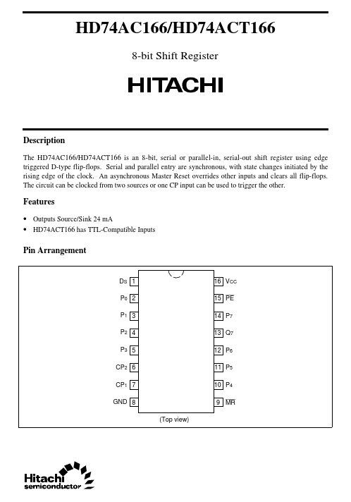
Pin Arrangement
DS 1 P0 2 P1 3 P2 4 P3 5 CP2 6 CP1 7 GND 8 (Top view)
16 VCC 15 PE 14 P7 13 Q7 12 P6 11 P5 10 P4 9 MR
HD74AC166/HD74ACT166
Logic Symbol
15 2 3 4 5 10 11 12 14
PE P0 P1 P2 P3 P4 P5 P6 P7 1 7 6 1 2 DS CP MR Q7
9
13 VCC=Pin16 GND=Pin8
Pin Names
CP1, CP2 DS PE P 0 to P7 MR Q7 Clock Pulse Inputs (Active Rising Edge) Serial Data Input Parallel Enable Input (Active Low) Parallel Data Inputs Asynchronous Master Reset Input (Active Low) Last Stage Output
Functional Description
Operation is synchronous (except for Master Reset) and state changes are initiated by the rising edge of either clock input if the other clock input is Low. When one of the clock inputs is used as an active High clock inhibt, it should attain the High state while the other clock is still in the High state following the previous operation. When the Parallel Enable ( PE ) input is Low, data is loaded into the register from the Parallel Data (P0 to P7) inputs on t...
Similar Datasheet