www.DataSheet4U.com
Pb Free Plating Product
ISSUED DATE :2006/03/28 REVISED DATE :
GTT2623
P-CHANNEL ENHANCEMENT MODE ...
www.DataSheet4U.com
Pb Free Plating Product
ISSUED DATE :2006/03/28 REVISED DATE :
GTT2623
P-CHANNEL ENHANCEMENT MODE POWER
MOSFET
BVDSS RDS(ON) ID
-30V 170m -2.0A
The GTT2623 utilized advanced processing techniques to achieve the lowest possible on-resistance, extremely efficient and cost-effectiveness device. The GTT2623 is universally used for all commercial-industrial applications.
Description
*Low Gate Charge *Low On-resistance
Features
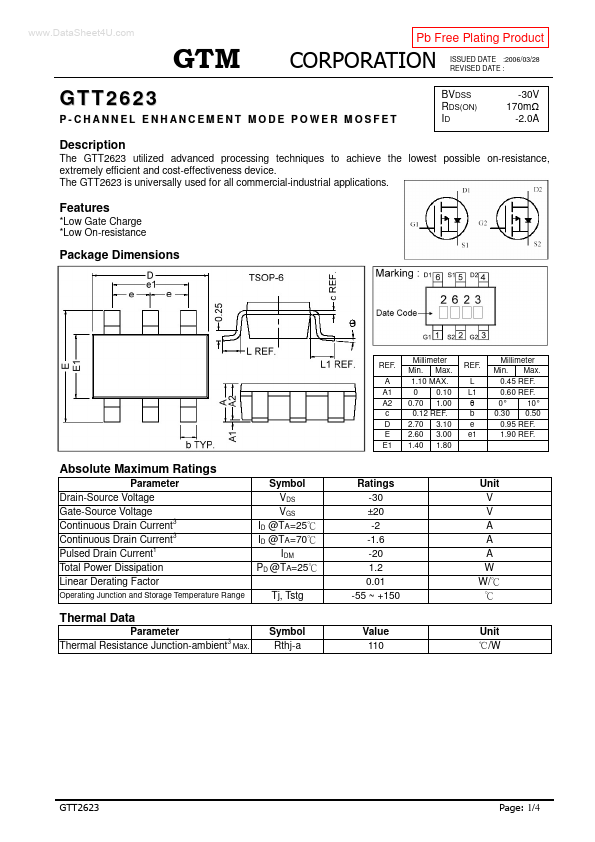
Package Dimensions
REF. A A1 A2 c D E E1
Millimeter Min. Max. 1.10 MAX. 0 0.10 0.70 1.00 0.12 REF. 2.70 3.10 2.60 3.00 1.40 1.80
REF. L L1 b e e1
Millimeter Min. Max. 0.45 REF. 0.60 REF. 0° 10° 0.30 0.50 0.95 REF. 1.90 REF.
Absolute Maximum Ratings
Parameter Drain-Source
Voltage Gate-Source
Voltage Continuous Drain Current3 3 Continuous Drain Current Pulsed Drain Current1 Total Power Dissipation Linear Derating Factor
Symbol VDS VGS ID @TA=25 ID @TA=70 IDM PD @TA=25 Tj, Tstg Symbol Rthj-a
Operating Junction and Storage Temperature Range
Ratings -30 ±20 -2 -1.6 -20 1.2 0.01 -55 ~ +150 Value 110
Unit V V A A A W W/
Thermal Data
Parameter Thermal Resistance Junction-ambient3 Max.
Unit /W
1/4
ISSUED DATE :2006/03/28 REVISED DATE :
Electrical Characteristics (Tj = 25
Parameter Drain-Source Breakdown
Voltage
Breakdown
Voltage Temperature Coefficient
unless otherwise specified)
Min. -30 -1.0 Typ. -0.02 2 2.8 0.5 1.4 5 6 15 3 150 42 32 Max. -3.0 ±100 -1 -25 170 280 4.5 240 pF ns nC Unit V V/ V S nA uA uA m Test Conditions...