www.DataSheet4U.com
Pb Free Plating Product
ISSUED DATE :2005/10/14 REVISED DATE :
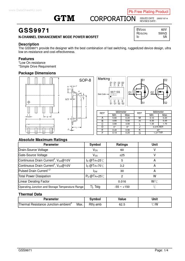
GSS9971
N-CHANNEL ENHANCEMENT MODE ...
www.DataSheet4U.com
Pb Free Plating Product
ISSUED DATE :2005/10/14 REVISED DATE :
GSS9971
N-CHANNEL ENHANCEMENT MODE POWER
MOSFET
BVDSS RDS(ON) ID
60V 50m 5A
The GSS9971 provide the designer with the best combination of fast switching, ruggedized device design, ultra low on-resistance and cost-effectiveness.
Description
Features
*Low On-resistance *Simple Drive Requirement
Package Dimensions
REF. A B C D E F
Millimeter Min. Max.
5.80 4.80 3.80 0° 0.40 0.19 6.20 5.00 4.00 8° 0.90 0.25
REF. M H L J K G
Millimeter Min. Max.
0.10 0.25 0.35 0.49 1.35 1.75 0.375 REF. 45° 1.27 TYP.
Absolute Maximum Ratings
Parameter Drain-Source
Voltage Gate-Source
Voltage Continuous Drain Current , VGS@10V Continuous Drain Current , VGS@10V Pulsed Drain Current
1,2 3 3
Symbol VDS VGS ID @TA=25 ID @TA=70 IDM PD @TA=25 Tj, Tstg
Ratings 60 ±25 5 3.2 30 2 0.016 -55 ~ +150
Unit V V A A A W W/
Total Power Dissipation Linear Derating Factor
Operating Junction and Storage Temperature Range
Thermal Data
Parameter Thermal Resistance Junction-ambient
3
Symbol Max. Rthj-amb
Value 62.5
Unit /W
GSS9971
Page: 1/4
ISSUED DATE :2005/10/14 REVISED DATE :
Electrical Characteristics(Tj = 25
Parameter Drain-Source Breakdown
Voltage
Breakdown
Voltage Temperature Coefficient
Unless otherwise specified)
Min. 60 1.0 Typ. 0.06 7 32.5 4.9 8.8 9.6 10 30 5.5 1658 156 109 Max. 3.0 ±100 1 25 50 60 pF ns nC Unit V V/ V S nA uA uA m Test Conditions VGS=0, ID=250uA Reference to 25 , ID=1mA VDS=VGS, ID=25...