www.DataSheet4U.com
ISSUED DATE :2005/12/23 REVISED DATE :
GSM BD2004
S U R F A C E M O U N T, S W I T C H I N G D I O ...
www.DataSheet4U.com
ISSUED DATE :2005/12/23 REVISED DATE :
GSM BD2004
S U R F A C E M O U N T, S W I T C H I N G D I O D E V O LT A G E 3 0 0 V, C U R R E N T 0 . 2 2 5 A
Description
The GSMBD2004 is designed for ultra high speed switching.
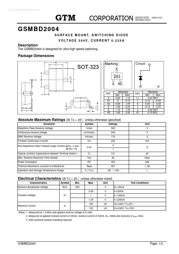
Package Dimensions
REF. A A1 A2 D E HE
Millimeter Min. Max. 0.80 1.10 0 0.10 0.80 1.00 1.80 2.20 1.15 1.35 1.80 2.40
REF. L1 L b c e Q1
Millimeter Min. Max. 0.42 REF. 0.15 0.35 0.25 0.40 0.10 0.25 0.65 REF. 0.15 BSC.
Absolute Maximum Ratings (At TA = 25
Parameter Repetitive Peak Reverse
Voltage Continuous reverse
voltage RMS Reverse
Voltage Forward Continuous Current Non-Repetitive Peak Forward surge Current @Tp =1.0us @Tp=1.0s Typical Junction Capacitance between Terminal (Note1) Max. Reverse Recovery Time (Note2) Power Dissipation Thermal Resistance Junction to Ambient Air Operation and Storage Temperature Range
unless otherwise specified)
Symbol VRRM VR(VRWM) VR(RMS) IFM IFSM CJ TRR PD R
JA
Ratings 300 240 170 225 4 1 5.0 50 350 357 -65 ~ +150
Unit V V V mA A pF nSec mW /W
TJ, TSTG
Electrical Characteristics (At TA = 25
Characteristics Reverse Breakdown
Voltage Forward
Voltage Symbol BVR VF Min. 300 Reverse Current IR -
unless otherwise noted)
Max. 0.85 1 1.25 100 100 Unit V V V V nA uA IR=100uA IF=20mA IF=100mA IF=225mA VR=240V, TA=25 VR=240V, TA=150 and recovery to IRR=-3mA. Test Conditions
Notes: 1. Measured at 1.0 MHz and applied reverse
voltage of 0 volts. 2. Measured at applied forward current of 30mA, reverse curr...