www.DataSheet4U.com
CORPORATION
GSD965
Description
NPN EPITAXIAL PLANAR T RANSISTOR
ISSUED DATE :2004/04/05 REVISED DA...
www.DataSheet4U.com
CORPORATION
GSD965
Description
NPN EPITAXIAL PLANAR T RANSISTOR
ISSUED DATE :2004/04/05 REVISED DATE :2004/11/29B
The GSD965 is designed for use as AF output amplifier and flash unit
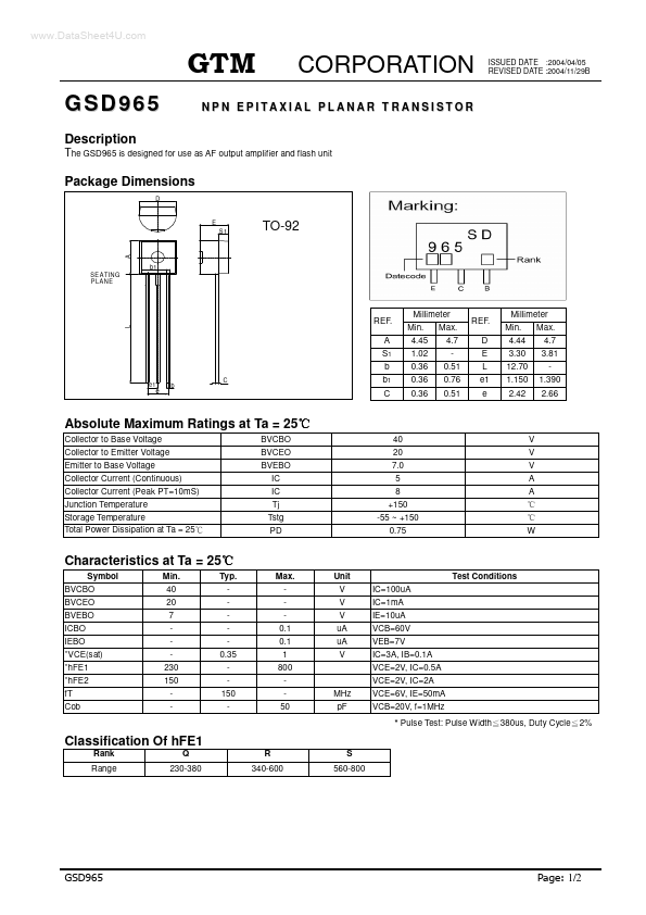
Package Dimensions
D E S1
TO-92
A
b1 SE A TING P LA NE
L
REF. A S1 b
e1 e b C
Millimeter Min. 4.45 1.02 0.36 0.36 0.36 Max. 4.7 0.51 0.76 0.51
REF. D E L e1 e
Millimeter Min. 4.44 3.30 12.70 1.150 2.42 Max. 4.7 3.81 1.390 2.66
b1 C
Absolute Maximum Ratings at Ta = 25
Collector to Base
Voltage Collector to Emitter
Voltage Emitter to Base
Voltage Collector Current (Continuous) Collector Current (Peak PT=10mS) Junction Temperature Storage Temperature Total Power Dissipation at Ta = 25 BVCBO BVCEO BVEBO IC IC Tj Tstg PD 40 20 7.0 5 8 +150 -55 ~ +150 0.75 W V V V A A
Characteristics at Ta = 25
Symbol BVCBO BVCEO BVEBO ICBO IEBO *VCE(sat) *hFE1 *hFE2 fT Cob Min. 40 20 7 230 150 Typ. 0.35 150 Max. 0.1 0.1 1 800 50 MHz pF Unit V V V uA uA V IC=100uA IC=1mA IE=10uA VCB=60V VEB=7V IC=3A, IB=0.1A VCE=2V, IC=0.5A VCE=2V, IC=2A VCE=6V, IE=50mA VCB=20V, f=1MHz * Pulse Test: Pulse Width 380us, Duty Cycle 2% Test Conditions
Classification Of hFE1
Rank Q Range 230-380
R 340-600
S 560-800
1/2
CORPORATION
Characteristics Curve
ISSUED DATE :2004/04/05 REVISED DATE :2004/11/29B
Important Notice: All rights are reserved. Reproduction in whole or in part is prohibited without the prior written approval of GTM. GTM reserves the right to make changes to its products without notic...