www.DataSheet4U.com
ISSUED DATE :2005/06/24 REVISED DATE :2005/10/05B
GSC4558
Description Features
D U A L O P E R AT ...
www.DataSheet4U.com
ISSUED DATE :2005/06/24 REVISED DATE :2005/10/05B
GSC4558
Description Features
D U A L O P E R AT I O N A L A M P L I F I E R
The GSC4558 is a monolithic integrated circuit designed for dual operational amplifier.
No frequency compensated required No latch-up Large common mode and differential
voltage range Parameter tracking over temperature range Gain and phase match between
amplifiers Internally frequency compensated Low noise input transistors
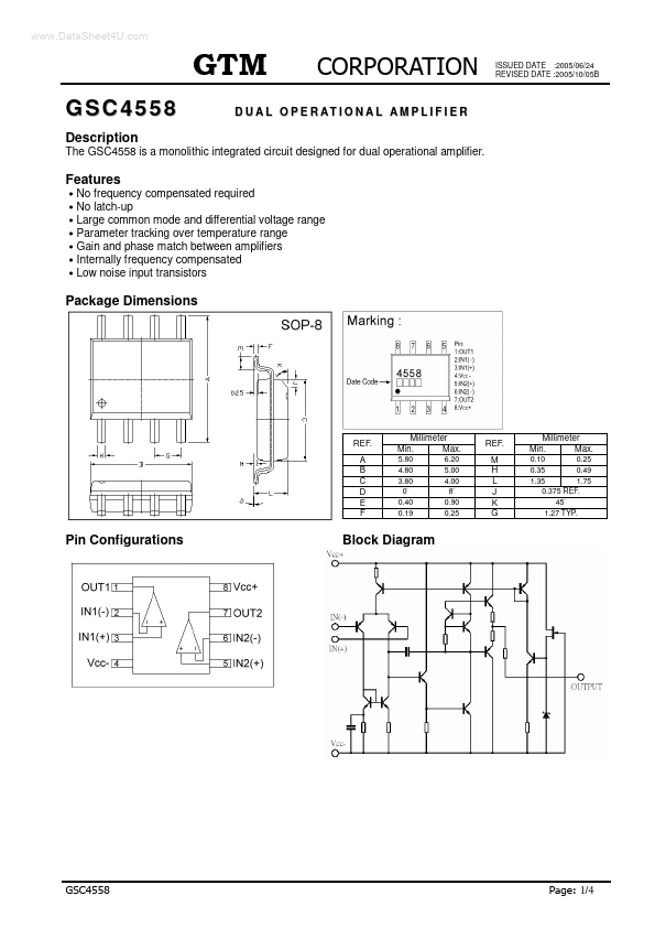
Package Dimensions
REF. A B C D E F
Millimeter Min. Max.
5.80 4.80 3.80 0 0.40 0.19 6.20 5.00 4.00 8 0.90 0.25
REF. M H L J K G
Millimeter Min. Max.
0.10 0.25 0.35 0.49 1.35 1.75 0.375 REF. 45 1.27 TYP.
Pin Configurations
Block Diagram
1/4
ISSUED DATE :2005/06/24 REVISED DATE :2005/10/05B
Absolute Maximum Ratings at Ta = 25
Parameter Supply
Voltage Differential Input
Voltage Input
Voltage Power Dissipation Operating Temperature Range Storage Temperature Range Symbol VCC VI(DIFF) VI PD TOPR TSTG Value ±22 ±18 ±15 400 0 ~ +70 -65 ~ +150 Unit V V V mW
Electrical Characteristics (VCC=15V Vee=-15V, TA=25 )
Parameter Supply Current, all Amp, no load Input Offset
Voltage Input Offset Current Input Bias Current Common Mode Input
Voltage Large Signal
Voltage Gain Output
Voltage Swing Common Mode Rejection Ratio Supply
Voltage Rejection Ratio Power Consumption Slew Rate Rise Time Overshoot Input Resistance Output Resistance Total Harmonic Distortion Channel Separation Symbol ICC VIO IIO IBIAS VI(R) GV VO(P-P...