www.DataSheet4U.com
Pb Free Plating Product
ISSUED DATE :2006/01/20 REVISED DATE :
GM2310
N-CHANNEL ENHANCEMENT MODE P...
www.DataSheet4U.com
Pb Free Plating Product
ISSUED DATE :2006/01/20 REVISED DATE :
GM2310
N-CHANNEL ENHANCEMENT MODE POWER
MOSFET
BVDSS RDS(ON) ID
60V 90m 3A
The GM2310 utilized advanced processing techniques to achieve the lowest possible on-resistance, extremely efficient and cost-effectiveness device. The GM2310 is universally used for all commercial-industrial surface mount applications.
Description
Features
*Simple Drive Requirement *Small Package Outline
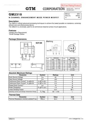
Package Dimensions SOT-89
REF. A B C D E F
Millimeter Min. Max. 4.4 4.6 4.05 4.25 1.50 1.70 1.30 1.50 2.40 2.60 0.89 1.20
REF. G H I J K L M
Millimeter Min. Max. 3.00 REF. 1.50 REF. 0.40 0.52 1.40 1.60 0.35 0.41 5° TYP. 0.70 REF.
Absolute Maximum Ratings
Parameter Drain-Source
Voltage Gate-Source
Voltage Continuous Drain Current3,
[email protected] 3 Continuous Drain Current ,
[email protected] 1,2 Pulsed Drain Current Power Dissipation Linear Derating Factor
Operating Junction and Storage Temperature Range
Symbol VDS VGS ID @TA=25 ID @TA=70 IDM PD @TA=25 Tj, Tstg Symbol Rthj-a
Ratings 60 ±20 3.0 2.3 10 1.5 0.01 -55 ~ +150 Value 83.3
Unit V V A A A W W/
Thermal Data
Parameter Thermal Resistance Junction-ambient3 Max. Unit /W
GM2310
Page: 1/4
www.DataSheet4U.com
ISSUED DATE :2006/01/20 REVISED DATE :
Electrical Characteristics (Tj = 25
Parameter Drain-Source Breakdown
Voltage
Breakdown
Voltage Temperature Coefficient
unless otherwise specified)
Min. 60 1.0 Typ. 0.05 5.0 6 1.6 3 6 5 16 3 490 55 40 Max. 3.0 ±100 10 25...