GFU30N03
New Product
Vishay Semiconductor
VDS 30V RDS(ON) 15mΩ ID 43A
N-Channel Enhancement-Mode MOSFET
H C N E ET R ...
GFU30N03
New Product
Vishay Semiconductor
VDS 30V RDS(ON) 15mΩ ID 43A
N-Channel Enhancement-Mode
MOSFET
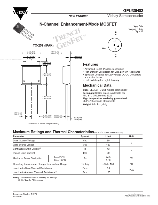
H C N E ET R T F N TO-251 (IPAK) E
0.265 (6.73) 0.255 (6.48) 0.214 (5.43) 0.206 (5.23) 0.094 (2.39) 0.087 (2.21)
D
TM
G
G
www.DataSheet4U.com
0.023 (0.58) 0.018 (0.46) 0.050 (1.27) 0.035 (0.89)
S
D
Features
Advanced Trench Process Technology High Density Cell Design for Ultra Low On-Resistance Specially Designed for Low
Voltage DC/DC Converters and motor drives Fast Switching for High Efficiency
0.245 (6.22) 0.235 (5.97)
G
S
Mechanical Data
0.375 (9.53) 0.350 (8.89)
Case: JEDEC TO-251 molded plastic body Terminals: Solder plated, solderable per MIL-STD-750, Method 2026 High temperature soldering guaranteed: 250°C/10 seconds at terminals Weight: 0.011oz., 0.4g
0.035 (0.89) 0.028 (0.71)
0.102 (2.59) 0.078 (1.98)
0.023 (0.58) 0.018 (0.46)
0.045 (1.14) 0.035 (0.89)
Dimensions in inches and (millimeters)
Maximum Ratings and Thermal Characteristics (T
Parameter Drain-Source
Voltage Gate-Source
Voltage Continuous Drain Current(1) Pulsed Drain Current Maximum Power Dissipation TC = 25°C TC = 100°C Symbol VDS VGS ID IDM PD TJ, Tstg RθJC
(2)
C
= 25°C unless otherwise noted)
Limit 30
± 20
Unit V
43 80 44.5 17.8 –55 to 150 2.8 125
A W °C °C/W
Operating Junction and Storage Temperature Range Junction-to-Case Thermal Resistance Junction-to-Ambient Thermal Resistance
RθJA
Note: (1) Maximum DC current limited by the package (2) 1-in2 2oz. Cu PCB moun...