www.DataSheet4U.com
CORPORATION
GD420SD
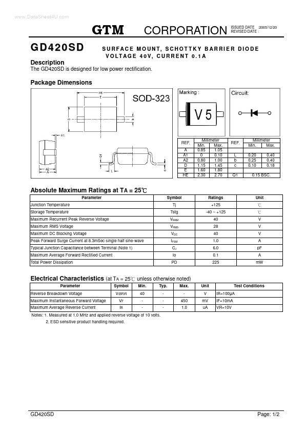
Description Package Dimensions
ISSUED DATE :2005/12/20 REVISED DATE :
S U R F...
www.DataSheet4U.com
CORPORATION
GD420SD
Description Package Dimensions
ISSUED DATE :2005/12/20 REVISED DATE :
S U R F A C E M O U N T, S C H O T T K Y B A R R I E R D I O D E V O LT A G E 4 0 V, C U R R E N T 0 . 1 A
The GD420SD is designed for low power rectification.
REF. A A1 A2 D E HE
Millimeter Min. Max. 0.85 1.05 0 0.10 0.80 1.00 1.15 1.45 1.60 1.80 2.30 2.70
REF. L b c Q1
Millimeter Min. Max. 0.20 0.25 0.10 0.40 0.40 0.18
0.15 BSC.
Absolute Maximum Ratings at TA = 25
Parameter Junction Temperature Storage Temperature Maximum Recurrent Peak Reverse
Voltage Maximum RMS
Voltage Maximum DC Blocking
Voltage Peak Forward Surge Current at 8.3mSec single half sine-wave Typical Junction Capacitance between Terminal (Note 1) Maximum Average Forward Rectified Current Total Power Dissipation Symbol Tj Tstg VRRM VRMS VDC IFSM CJ Io PD Ratings +125 -40 ~ +125 40 28 40 1.0 6.0 0.1 225 V V V A pF A mW Unit
Electrical Characteristics (at TA = 25
Parameter Reverse Breakdown
Voltage Maximum Instantaneous Forward
Voltage Maximum Average Reverse Current Symbol V(BR)R VF IR
unless otherwise noted)
Min. 40 Typ. Max. 450 1.0 Unit V mV uA IF=10mA VR=10V Test Conditions IR=100 A
Notes: 1. Measured at 1.0 MHz and applied reverse
voltage of 10 volts. 2. ESD sensitive product handling required.
GD420SD
Page: 1/2
CORPORATION
Characteristics Curve
ISSUED DATE :2005/12/20 REVISED DATE :
Important Notice: All rights are reserved. Reproduction in whole or in part is prohibited without...