www.DataSheet4U.com
G B AT 5 4 / A / C / S
Description
Silicon Schottky Barrier Double Diodes .
1/2
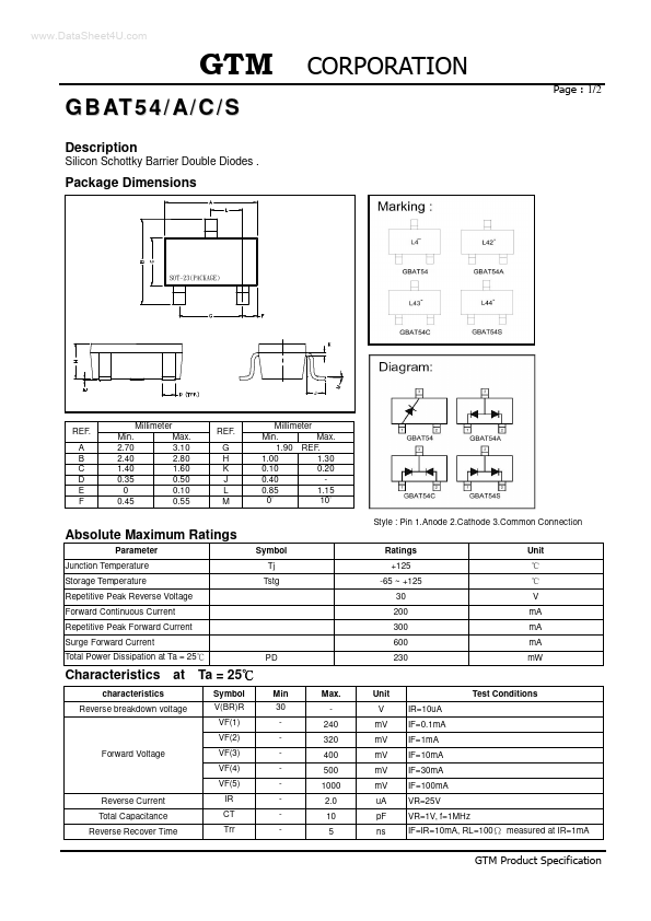
Package Dimension...
www.DataSheet4U.com
G B AT 5 4 / A / C / S
Description
Silicon Schottky Barrier Double Diodes .
1/2
Package Dimensions
REF. A B C D E F
Min. 2.70 2.40 1.40 0.35 0 0.45
Millimeter
Max. 3.10 2.80 1.60 0.50 0.10 0.55
REF. G H K J L M
Millimeter Min. Max. 1.90 REF. 1.00 1.30 0.10 0.20 0.40 0.85 1.15 0 10 Style : Pin 1.Anode 2.Cathode 3.Common Connection Symbol Tj Tstg Ratings +125 -65 ~ +125 30 200 300 600 PD 230 V mA mA mA mW Unit
Absolute Maximum Ratings
Parameter Junction Temperature Storage Temperature Repetitive Peak Reverse
Voltage Forward Continuous Current Repetitive Peak Forward Current Surge Forward Current Total Power Dissipation at Ta = 25
Characteristics
characteristics
at Ta = 25
Symbol V(BR)R VF(1) VF(2) Min 30 Max. 240 320 400 500 1000 2.0 10 5 Unit V mV mV mV mV mV uA pF ns IR=10uA IF=0.1mA IF=1mA IF=10mA IF=30mA IF=100mA VR=25V VR=1V, f=1MHz IF=IR=10mA, RL=100 measured at IR=1mA Test Conditions
Reverse breakdown
voltage
Forward
Voltage
VF(3) VF(4) VF(5) IR CT Trr
Reverse Current Total Capacitance Reverse Recover Time
2/2
Characteristics Curve
Important Notice: All rights are reserved. Reproduction in whole or in part is prohibited without the prior written approval of GTM. GTM reserves the right to make changes to its products without notice. GTM semiconductor products are not warranted to be suitable for use in life-support Applications, or systems. GTM assumes no liability for any consequence of customer product design, infringement of paten...