www.DataSheet4U.com
G 4 11 S D
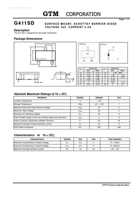
Description Package Dimensions
1/2 S U R F A C E M O U N T, S C H O T T K Y B A R R I E...
www.DataSheet4U.com
G 4 11 S D
Description Package Dimensions
1/2 S U R F A C E M O U N T, S C H O T T K Y B A R R I E R D I O D E V O LT A G E 4 0 V, C U R R E N T 0 . 5 A
The G411SD is designed for low power rectification
REF. A B C D E F
Millimeter Min. Max. 2.70 3.10 2.40 2.80 1.40 1.60 0.35 0.50 0 0.10 0.45 0.55
REF. G H K J L M
Millimeter Min. Max. 1.90 REF. 1.00 1.30 0.10 0.20 0.40 0.85 1.15 0 10
Absolute Maximum Ratings at Ta = 25
Parameter Junction Temperature Storage Temperature Maximum Recurrent Peak Reverse
Voltage Maximum RMS
Voltage Maximum DC Blocking
Voltage Peak Forward Surge Current at 8.3mSec single half sine-wave Typical Junction Capacitance between Terminal Maximum Average Forward Rectified Current Total Power Dissipation Symbol Tj Tstg VRRM VRMS VDC IFSM CJ Io PD Ratings +125 -40 ~ +125 40 28 20 3 20 0.5 225 V V V A pF A mW Unit
Characteristics
at Ta = 25
Symbol VF(1) VF(2) IR Typ. 0.3 0.5 30 Unit V V uA Test Condition IF = 10mA IF =500mA VR = 10V
Characteristics Maximum Instantaneous Forward
Voltage Maximum Instantaneous Forward
Voltage Maximum Average Reverse Current
2/2
Characteristics Curve
Important Notice: All rights are reserved. Reproduction in whole or in part is prohibited without the prior written approval of GTM. GTM reserves the right to make changes to its products without notice. GTM semiconductor products are not warranted to be suitable for use in life-support Applications, or systems. GTM assumes no liability for any conse...