www.DataSheet4U.com
Pb Free Plating Product
CORPORATION
G3407
P-CHANNEL ENHANCEMENT MODE POWER MOSFET
ISSUED DATE :20...
www.DataSheet4U.com
Pb Free Plating Product
CORPORATION
G3407
P-CHANNEL ENHANCEMENT MODE POWER
MOSFET
ISSUED DATE :2007/01/15 REVISED DATE :
BVDSS RDS(ON) ID
-30V 52m -4.1A
Description
The G3407 uses advanced trench technology to provide excellent on-resistance with low gate change. The device is suitable for use as a load switch or in PWM applications. *Lower Gate Charge *Small Package Outline *RoHS Compliant
Features
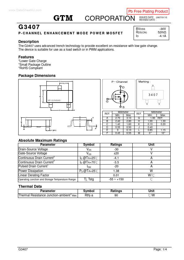
Package Dimensions
REF. A B C D E F
Millimeter Min. Max. 2.70 3.10 2.40 2.80 1.40 1.60 0.35 0.50 0 0.10 0.45 0.55
REF. G H K J L M
Millimeter Min. Max. 1.90 REF. 1.00 1.30 0.10 0.20 0.40 0.85 1.15 0° 10°
Absolute Maximum Ratings
Parameter Drain-Source
Voltage Gate-Source
Voltage 3 Continuous Drain Current 3 Continuous Drain Current 1 Pulsed Drain Current Power Dissipation Linear Derating Factor
Operating Junction and Storage Temperature Range
Symbol VDS VGS ID @TA=25 ID @TA=70 IDM PD @TA=25 Tj, Tstg Symbol Rthj-a
Ratings -30 ±20 -4.1 -3.5 -20 1.38 0.01 -55 ~ +150 Ratings 90
Unit V V A A A W W/
Thermal Data
Parameter 3 Thermal Resistance Junction-ambient Max. Unit /W
G3407
Page: 1/4
CORPORATION
Electrical Characteristics (Tj = 25
Parameter Drain-Source Breakdown
Voltage Gate Threshold
Voltage Forward Transconductance Gate-Source Leakage Current
Drain-Source Leakage Current(Tj=25 ) Drain-Source Leakage Current(Tj=55 )
ISSUED DATE :2007/01/15 REVISED DATE :
unless otherwise specified)
Min. -30 -1.0 Typ. 8.2 7 3.1 3 8.6 5 28.2 13.5 700 120 75...