G2N7002
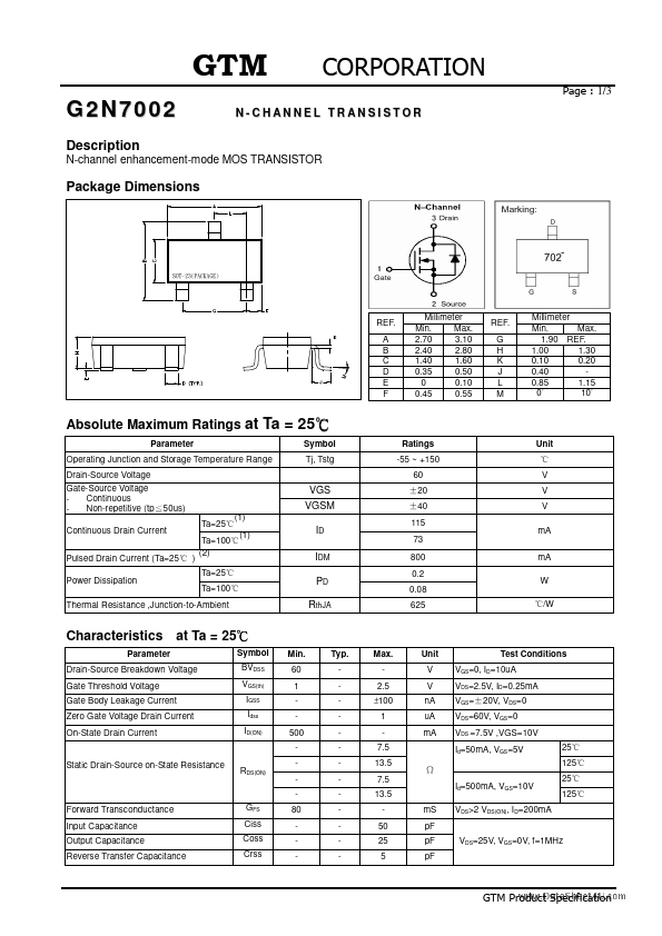
Description Package Dimensions
1/3 N-CHANNEL TRANSISTOR
N-channel enhancement-mode MOS TRANSISTOR
REF. A B C ...
G2N7002
Description Package Dimensions
1/3 N-CHANNEL TRANSISTOR
N-channel enhancement-mode MOS TRANSISTOR
REF. A B C D E F
Millimeter Min. Max. 2.70 3.10 2.40 2.80 1.40 1.60 0.35 0.50 0 0.10 0.45 0.55
REF. G H K J L M
Millimeter Min. Max. 1.90 REF. 1.00 1.30 0.10 0.20 0.40 0.85 1.15 0 10
Absolute Maximum Ratings at Ta = 25
Parameter Operating Junction and Storage Temperature Range Drain-Source
Voltage Gate-Source
Voltage Continuous Non-repetitive (tp 50us) Continuous Drain Current Pulsed Drain Current (Ta=25 Power Dissipation ) Ta=25 Ta=100 (2) Ta=25 Ta=100 Symbol Tj, Tstg Ratings -55 ~ +150 60 V V V mA mA W /W 20 40 115 73 800 0.2 0.08 625 Unit
VGS VGSM
(1) (1)
ID IDM PD RthJA
Thermal Resistance ,Junction-to-Ambient
Characteristics
Parameter
at Ta = 25
Symbol BVDSS VGS(th) IGSS Idss ID(ON) Min. 60 1 500 80 Typ. Max. 2.5 100 1 7.5 13.5 7.5 13.5 50 25 5 mS pF pF pF VDS=25V, VGS =0V, f=1MHz Id=500mA, VGS=10V VDS>2 VDS(ON), ID=200mA Unit V V nA uA mA Test Conditions VGS=0, ID=10uA VDS=2.5V, ID=0.25mA VGS= 20V, VDS=0 VDS=60V, VGS=0 VDS =7.5V ,VGS=10V Id=50mA, VGS =5V 25 125 25 125
Drain-Source Breakdown
Voltage Gate Threshold
Voltage Gate Body Leakage Current Zero Gate
Voltage Drain Current On-State Drain Current
Static Drain-Source on-State Resistance
RDS(ON)
Forward Transconductance Input Capacitance Output Capacitance Reverse Transfer Capacitance
GFS Ciss Coss Crss
2/3
(1)The Power Dissipation of the package may result in a continuous train current. (2)Pulse ...