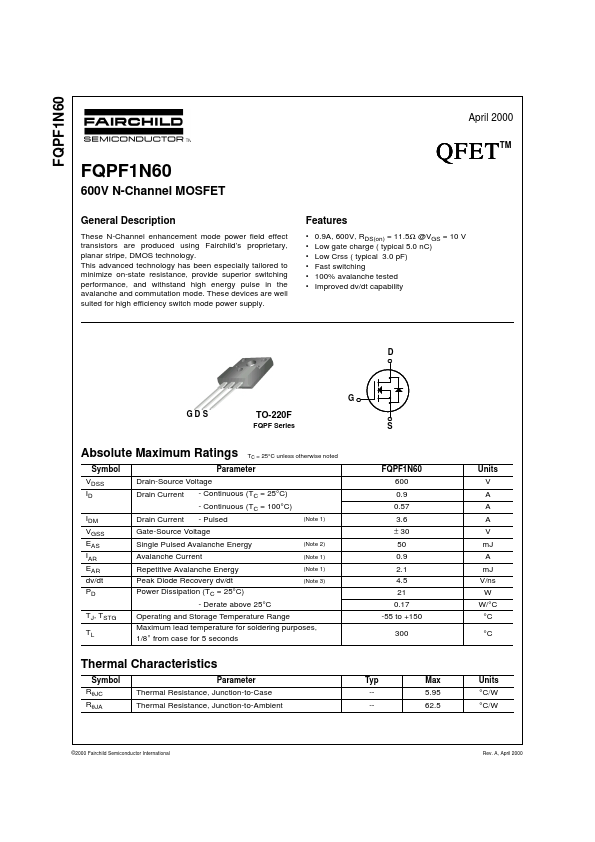
DatasheetsPDF.com

FQPF1N60 Datasheet

Part Number FQPF1N60
Manufacturers Fairchild Semiconductor
Logo Fairchild Semiconductor
Description 600V N-Channel MOSFET
Datasheet FQPF1N60 DatasheetFQPF1N60 Datasheet (PDF)

  FQPF1N60   FQPF1N60
FQPF1N60 April 2000 QFET FQPF1N60 600V N-Channel MOSFET General Description These N-Channel enhancement mode power field effect transistors are produced using Fairchild’s proprietary, planar stripe, DMOS technology. This advanced technology has been especially tailored to minimize on-state resistance, provide superior switching performance, and withstand high energy pulse in the avalanche and commutation mode. These devices are well suited for high efficiency switch mode power supply. TM Features • • • • • • 0.9A, 600V, RDS(on) = 11.5Ω @VGS = 10 V Low gate charge ( typical 5.0 nC) Low Crss ( typical 3.0 pF) Fast switching 100% avalanche tested Improved dv/dt capability D ! " G! GD S ! " " " TO-220F FQPF Series ! S Absolute Maximum Ratings Symbol VDSS ID IDM VGSS EAS IAR EAR dv/dt PD TJ, TSTG TL TC = 25°C unless otherwise noted Parameter Drain-Source Voltage - Continuous (TC = 25°C) Drain Current - Continuous (TC = 100°C) Drain Current - Pulsed (Note 1) FQPF1N60 600 0.9 .


600V N-Channel MOSFET

FQPF1N60 April 2000 QFET FQPF1N60 600V N-Channel MOSFET General Description These N-Channel enhancement mode power field effect transistors are produced using Fairchild’s proprietary, planar stripe, DMOS technology. This advanced technology has been especially tailored to minimize on-state resistance, provide superior switching performance, and withstand high energy pulse in the avalanche and commutation mode. These devices are well suited for high efficiency switch mode power supply. TM Features • • • • • • 0.9A, 600V, RDS(on) = 11.5Ω @VGS = 10 V Low gate charge ( typical 5.0 nC) Low Crss ( typical 3.0 pF) Fast switching 100% avalanche tested Improved dv/dt capability D ! " G! GD S ! " " " TO-220F FQPF Series ! S Absolute Maximum Ratings Symbol VDSS ID IDM VGSS EAS IAR EAR dv/dt PD TJ, TSTG TL TC = 25°C unless otherwise noted Parameter Drain-Source Voltage - Continuous (TC = 25°C) Drain Current - Continuous (TC = 100°C) Drain Current - Pulsed (Note 1) FQPF1N60 600 0.9 0.57 3.6 ±30 (Note 2) (Note 1) (Note 1) (Note 3) Units V A A A V mJ A mJ V/ns W W/°C °C °C Gate-Source Voltage Single Pulsed Avalanche Energy Avalanche Current Repetitive Avalanche Energy Peak Diode Recovery dv/dt Power Dissipation (TC = 25°C) 50 0.9 2.1 4.5 21 0.17 -55 to +150 300 - Derate above 25°C Operating and Storage Temperature Range Maximum lead temperature for soldering purposes, 1/8 from case for 5 seconds Thermal Characteristics Symbol RθJC RθJA Parameter Thermal Resistance, Ju.


2005-04-01 : R2KY    M28F008    M28F010    M28F512    M27C516    M27C64    M27C64A    M27C800    M27V101    M27V102   


@ 2014 :: Datasheetspdf.com ::
Semiconductors datasheet search & download site (Privacy Policy & Contact)