FQD6N50C / FQU6N50C
QFET
FQD6N50C / FQU6N50C
500V N-Channel MOSFET
General Description
These N-Channel enhancement mode...
FQD6N50C / FQU6N50C
QFET
FQD6N50C / FQU6N50C
500V N-Channel
MOSFET
General Description
These N-Channel enhancement mode power field effect transistors are produced using Fairchild’s proprietary, planar stripe, DMOS technology. This advanced technology has been especially tailored to minimize on-state resistance, provide superior switching performance, and withstand high energy pulse in the avalanche and commutation mode. These devices are well suited for high efficiency switched mode power supplies, active power factor correction, electronic lamp ballasts based on half bridge topology.
®
Features
4.5A, 500V, RDS(on) = 1.2 Ω @VGS = 10 V Low gate charge (typical 19nC) Low Crss (typical 15pF) Fast switching 100% avalanche tested Improved dv/dt capability
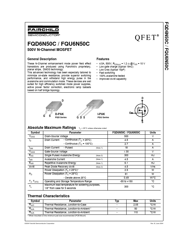
D D
!
●
◀
▲
● ●
G
S
D-PAK
FQD Series
I-PAK
G D S
FQU Series
G!
!
S
Absolute Maximum Ratings
Symbol VDSS ID IDM VGSS EAS IAR EAR dv/dt PD TJ, TSTG TL
TC = 25°C unless otherwise noted
Parameter Drain-Source
Voltage - Continuous (TC = 25°C) Drain Current - Continuous (TC = 100°C) Drain Current - Pulsed
(Note 1)
FQD6N50C / FQU6N50C 500 4.5 2.7 18 ± 30
(Note 2) (Note 1) (Note 1) (Note 3)
Units V A A A V mJ A mJ V/ns W W W/°C °C °C
Gate-Source
Voltage Single Pulsed Avalanche Energy Avalanche Current Repetitive Avalanche Energy Peak Diode Recovery dv/dt Power Dissipation (TA = 25°C)* Power Dissipation (TC = 25°C) - Derate above 25°C Operating and Storage Temperature Range Maximum lead temperature for sold...