PRELIMINARY
• FEATURES (1.8 GHz) ♦ 31 dBm Linear Output Power ♦ 16 dB Power Gain ♦ Useable Gain to 10 GHz ♦ 41 dBm Outpu...
PRELIMINARY
FEATURES (1.8 GHz) ♦ 31 dBm Linear Output Power ♦ 16 dB Power Gain ♦ Useable Gain to 10 GHz ♦ 41 dBm Output IP3 ♦ Maximum Stable Gain of 20 dB ♦ 50% Power-Added Efficiency ♦ 10V Operation / Plated Source Thru-Vias
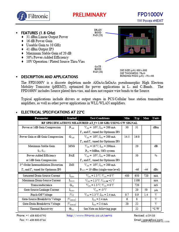
DRAIN BOND PAD (2X)
FPD1000V
1W POWER PHEMT
GATE BOND PAD (2X)
DESCRIPTION AND APPLICATIONS
DIE SIZE (µm): 650 x 800 DIE THICKNESS: 75µm BONDING PADS (µm): >70 x 65
The FPD1000V is a discrete depletion mode AlGaAs/InGaAs pseudomorphic High Electron Mobility Transistor (pHEMT), optimized for power applications in L- and C-Bands. The FPD1000V includes Source plated thru-vias, and does not require wire bonds to the Source. Typical applications include drivers or output stages in PCS/Cellular base station transmitter
amplifiers, as well as other power applications in WLL/WLAN
amplifiers.
ELECTRICAL SPECIFICATIONS AT 22°C
Parameter Power at 1dB Gain Compression Power Gain at dB Gain Compression Maximum Stable Gain S21/S12 Power-Added Efficiency at 1dB Gain Compression 3 -Order Intermodulation Distortion ΓS and ΓL tuned for Optimum IP3 Saturated Drain-Source Current Maximum Drain-Source Current Transconductance Gate-Source Leakage Current Pinch-Off
Voltage Gate-Source Breakdown
Voltage Gate-Drain Breakdown
Voltage Thermal Resistivity IDSS IMAX GM IGSO |VP| |VBDGS| |VBDGD| ΘCC
rd
Symbol P1dB G1dB MSG PAE IM3
Test Conditions VDS = 10V; IDS = 200 mA ΓS and ΓL tuned for Optimum IP3 VDS = 10V; IDS = 200 mA ΓS and ΓL tuned for Optimum IP3 VDS = 10 V; ...