FDS8896 N-Channel PowerTrench® MOSFET
April 2005
FDS8896 N-Channel PowerTrench® MOSFET
30V, 15A, 6.0mΩ Features
r DS(O...
FDS8896 N-Channel PowerTrench®
MOSFET
April 2005
FDS8896 N-Channel PowerTrench®
MOSFET
30V, 15A, 6.0mΩ Features
r DS(ON) = 6.0mΩ, VGS = 10V, ID = 15A r DS(ON) = 7.3mΩ, V GS = 4.5V, ID = 14A High performance trench technology for extremely low r DS(ON) Low gate charge High power and current handling capability
General Description
This N-Channel
MOSFET has been designed specifically to improve the overall efficiency of DC/DC converters using either synchronous or conventional switching PWM controllers. It has been optimized for low gate charge, low r DS(ON) and fast switching speed.
Applications
DC/DC converters
www.DataSheet4U.com
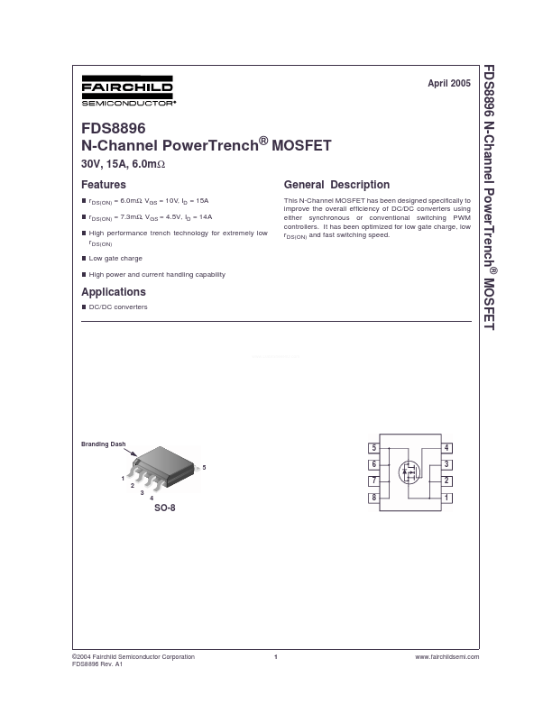
Branding Dash
5
5
4 3 2 1
6 7
1 2 3 4
8
SO-8
©2004 Fairchild Semiconductor Corporation FDS8896 Rev. A1
1
www.fairchildsemi.com
FDS8896 N-Channel PowerTrench®
MOSFET
MOSFET Maximum Ratings TA = 25°C unless otherwise noted
Symbol VDSS VGS Parameter Drain to Source
Voltage Gate to Source
Voltage Drain Current ID Continuous (TA = 25oC, VGS = 10V, R θJA = 50oC/W) Continuous (TA = 25 C, VGS = 4.5V, Rθ JA = 50 C/W) Pulsed EAS PD TJ, TSTG Single Pulse Avalanche Energy (Note 1) Power dissipation Derate above 25oC Operating and Storage Temperature
o o
Ratings 30 ±20 15 14 Figure 4 196 2.5 20 -55 to 150
Units V V A A A mJ W mW/oC
o
C
Thermal Characteristics
Rθ JC Rθ JA Rθ JA Thermal Resistance, Junction to Case (Note 2) Thermal Resistance, Junction to Ambient at 10 seconds (Note 3) Thermal Resistance, Junction to Ambient at 1000 seconds (No...