FDS6982AS
FDS6982AS
Dual Notebook Power Supply N-Channel PowerTrench® SyncFET™
General Description
The FDS6982AS is de...
FDS6982AS
FDS6982AS
Dual Notebook Power Supply N-Channel PowerTrench® SyncFET™
General Description
The FDS6982AS is designed to replace two single SO8
MOSFETs and Schottky diode in synchronous DC:DC power supplies that provide various peripheral
voltages for notebook computers and other battery powered electronic devices. FDS6982AS contains two unique 30V, N-channel, logic level, PowerTrench
MOSFETs designed to maximize power conversion efficiency. The high-side switch (Q1) is designed with specific emphasis on reducing switching losses while the low-side switch (Q2) is optimized to reduce conduction losses. Q2 also includes an integrated Schottky diode using ON Semiconductor’s monolithic SyncFET technology.
Applications
Notebook
Features
Q2: Optimized to minimize conduction losses Includes SyncFET Schottky body diode
8.6A, 30V
RDS(on) max= 13.5mΩ @ VGS = 10V RDS(on) max= 16.5mΩ @ VGS = 4.5V
Low gate charge (21nC typical)
Q1: Optimized for low switching losses
6.3A, 30V
RDS(on) max= 28.0mΩ @ VGS = 10V RDS(on) max= 35.0mΩ @ VGS = 4.5V
Low gate charge (11nC typical)
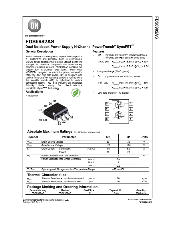
D1 D1 D2
D2
SO-8
G1 S1 G2 S2
5
4
6
Q1
3
7
2
Q2
8
1
Absolute Maximum Ratings TA = 25°C unless otherwise noted
Symbol
Parameter
VDSS VGSS ID PD
TJ, TSTG
Drain-Source
Voltage Gate-Source
Voltage
Drain Current - Continuous - Pulsed
Power Dissipation for Dual Operation Power Dissipation for Single Operation
(Note 1a)
(Note 1a) (Note 1b)
(Note 1c)
Operating and Storage Junction Te...