FDS6912
January 2000
FDS6912
Dual N-Channel Logic Level PWM Optimized PowerTrench MOSFET
General Description
These N-...
FDS6912
January 2000
FDS6912
Dual N-Channel Logic Level PWM Optimized PowerTrench
MOSFET
General Description
These N-Channel Logic Level
MOSFETs have been designed specifically to improve the overall efficiency of DC/DC converters using either synchronous or conventional switching PWM controllers. These
MOSFETs feature faster switching and lower gate charge than other
MOSFETs with comparable RDS(ON) specifications. The result is a
MOSFET that is easy and safer to drive (even at very high frequencies), and DC/DC power supply designs with higher overall efficiency.
Features
RDS(ON) = 0.028 Ω @ VGS = 10 V 6 A, 30 V. RDS(ON) = 0.042 Ω @ VGS = 4.5 V. Optimized for use in switching DC/DC converters with PWM controllers Very fast switching. Low gate charge
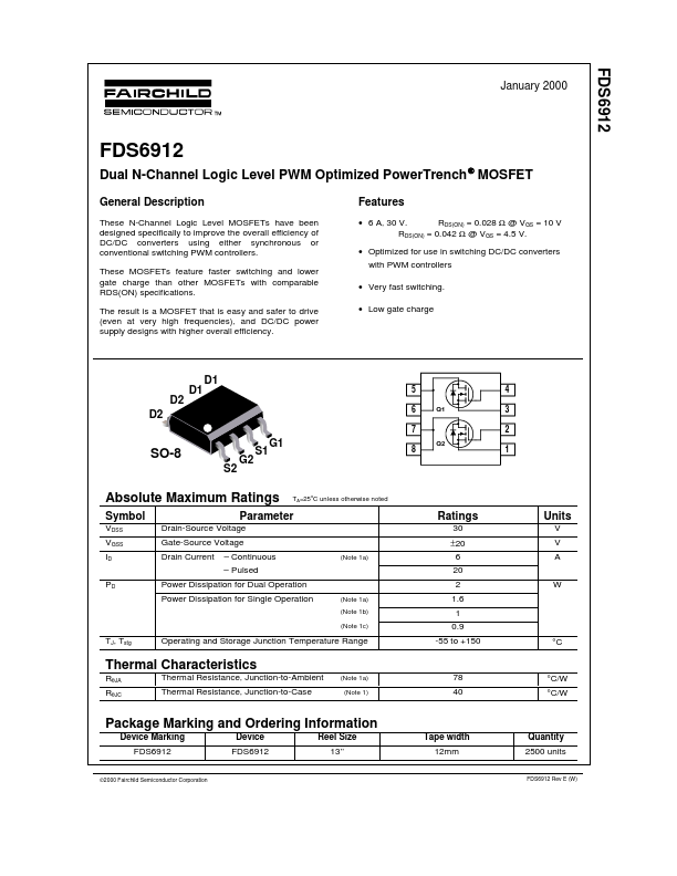
D1 D1 D2 D2 S1 G1
5 6 7
Q1
4 3 2
Q2
SO-8
S2
8
1
G2
Absolute Maximum Ratings
Symbol
VDSS VGSS ID PD Drain-Source
Voltage Gate-Source
Voltage Drain Current – Continuous – Pulsed
TA=25 C unless otherwise noted
o
Parameter
Ratings
30 ±20
(Note 1a)
Units
V V A W
6 20 2
Power Dissipation for Dual Operation Power Dissipation for Single Operation
(Note 1a) (Note 1b) (Note 1c)
1.6 1 0.9 -55 to +150 °C
TJ, Tstg
Operating and Storage Junction Temperature Range
Thermal Characteristics
RθJA RθJC Thermal Resistance, Junction-to-Ambient Thermal Resistance, Junction-to-Case
(Note 1a) (Note 1)
78 40
°C/W °C/W
Package Marking and Ordering Information
Device Marking FDS6912
2000 Fairchild Semiconductor Corporation
...