FDM2452NZ
July 2005
FDM2452NZ
Monolithic Common Drain N-Channel 2.5V Specified PowerTrench® MOSFET
General Description...
FDM2452NZ
July 2005
FDM2452NZ
Monolithic Common Drain N-Channel 2.5V Specified PowerTrench®
MOSFET
General Description
This dual N-Channel
MOSFET has been designed using Fairchild Semiconductor’s advanced Power Trench process to optimize the RDS(ON) @ VGS = 2.5v on special MicroFET lead frame with all the drains on one side of the package.
Features
8.1 A, 30 V RDS(ON) = 21 mΩ @ VGS = 4.5 V RDS(ON) = 25 mΩ @ VGS = 2.5 V ESD protection Diode(note 3) Low Profile – 0.8 mm maximum – in the new package MicroFET 2 x 5 mm
Applications
Li-Ion Battery Pack
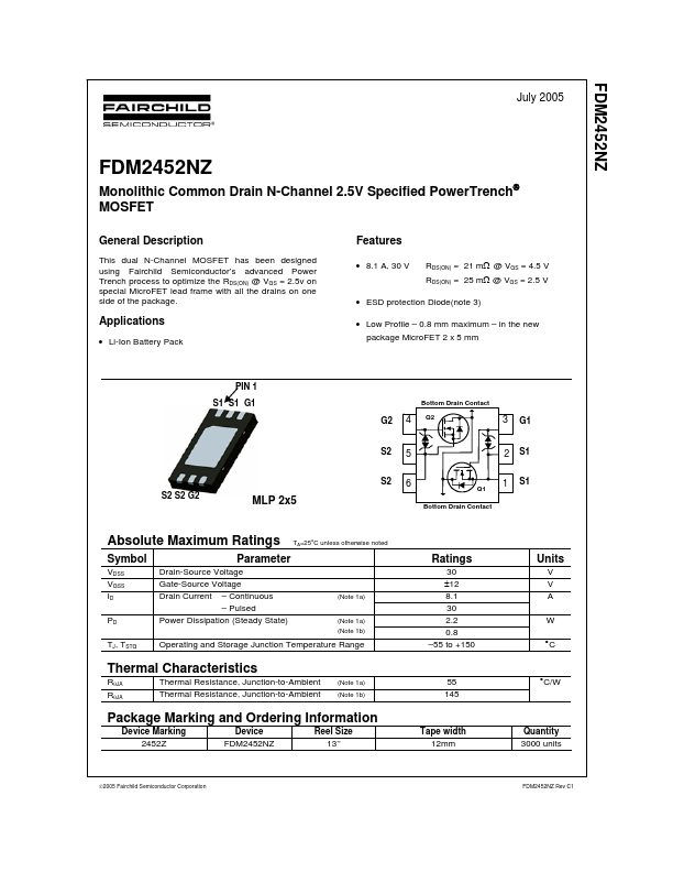
PIN 1 S1 S1 G1 G2
Bottom Drain Contact
4
Q2
3
G1
S2
5 6
2 1
S1
S2 S2 S2 G2
Q1 Bottom Drain Contact
S1
MLP 2x5
Absolute Maximum Ratings
Symbol
VDSS VGSS ID PD TJ, TSTG
TA=25oC unless otherwise noted
Parameter
Drain-Source
Voltage Gate-Source
Voltage Drain Current – Continuous – Pulsed Power Dissipation (Steady State)
Ratings
30 ±12 8.1 30 2.2 0.8 –55 to +150
Units
V V A W °C
(Note 1a)
(Note 1a) (Note 1b)
Operating and Storage Junction Temperature Range
Thermal Characteristics
RθJA RθJA Thermal Resistance, Junction-to-Ambient Thermal Resistance, Junction-to-Ambient
(Note 1a) (Note 1b)
55 145
°C/W
Package Marking and Ordering Information
Device Marking 2452Z Device FDM2452NZ Reel Size 13’’ Tape width 12mm Quantity 3000 units
©2005 Fairchild Semiconductor Corporation
FDM2452NZ Rev C1
FDM2452NZ
Electrical Characteristics
Symbol
BVDSS ∆BVDSS ∆TJ IDSS IGSS VGS(th) ∆VGS(th) ∆TJ RDS(on)
TA = 25°C unle...