MOSFET – P-Channel, POWERTRENCH) Integrated with Schottky Diode
-20 V, -3.1 A, 95 mW
FDFMA2P029Z, FDFMA2P029Z-F106
Gener...
MOSFET – P-Channel, POWERTRENCH) Integrated with Schottky Diode
-20 V, -3.1 A, 95 mW
FDFMA2P029Z, FDFMA2P029Z-F106
General Description This device is designed specifically as a single package solution for
the battery charge switch in cellular handset and other ultra−portable applications. It features a
MOSFET with very low on−state resistance and an independently connected low forward
voltage schottky diode allows for minimum conduction losses.
The MicroFET t 2X2 package offers exceptional thermal performance for its physical size and is well suited to linear mode applications.
Features
MOSFET
Max rDS(on) = 95 mW at VGS = –4.5 V, ID = –3.1 A Max rDS(on) = 141 mW at VGS = –2.5 V, ID = –2.5 A HBM ESD Protection Level > 2.5 kV (Note 1)
Schottky
VF < 0.37 V @ 500 mA Low Profile − 0.8 mm Maximum − In the New Package MicroFET
2x2 mm
These Devices are Pb−Free and are RoHS Compliant
NOTE: 1. The diode connected between the gate and source serves only
protection against ESD. No gate over
voltage rating is implied.
DATA SHEET www.onsemi.com
VDS MAX −20 V
MOSFET rDS(on) MAX 95 mW @ −4.5 V 141 mW @ −2.5 V
ID MAX −3.1 A
SCHOTTKY DIODE
VRRM MAX
VF MAX
20 V
0.37 V @ 500 mA
IO MAX 2A
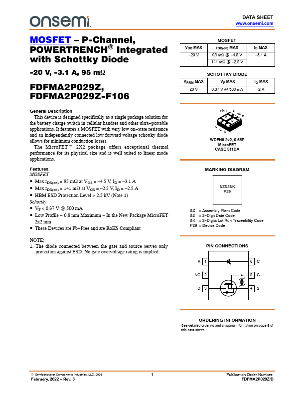
Pin 1 C
A NC D
D
C G S
WDFN6 2x2, 0.65P MicroFET
CASE 511DA
MARKING DIAGRAM
&Z&2&K P29
&Z = Assembly Plant Code &2 = 2−Digit Date Code &K = 2−Digits Lot Run Traceability Code P29 = Device Code
PIN CONNECTIONS
A1 NC 2
D3
6C 5G 4S
ORDERING INFORMATION
See detailed ordering and shippin...