FDD8424H Dual N & P-Channel PowerTrench® MOSFET
March 2007
FDD8424H
Dual N & P-Channel PowerTrench® MOSFET
Features
Q1...
FDD8424H Dual N & P-Channel PowerTrench®
MOSFET
March 2007
FDD8424H
Dual N & P-Channel PowerTrench®
MOSFET
Features
Q1: N-Channel Max rDS(on) = 24mΩ at VGS = 10V, ID = 9.0A Max rDS(on) = 30mΩ at VGS = 4.5V, ID = 7.0A Q2: P-Channel Max rDS(on) = 54mΩ at VGS = -10V, ID = -6.5A Max rDS(on) = 70mΩ at VGS = -4.5V, ID = -5.6A Fast switching speed RoHS Compliant
tm
N-Channel: 40V, 20A, 24mΩ P-Channel: -40V, -20A, 54mΩ
General Description
These dual N and P-Channel enhancement mode Power
MOSFETs are produced using Fairchild Semiconductor’s advanced PowerTrench- process that has been especially tailored to minimize on-state resistance and yet maintain superior switching performance.
Application
Inverter H-Bridge
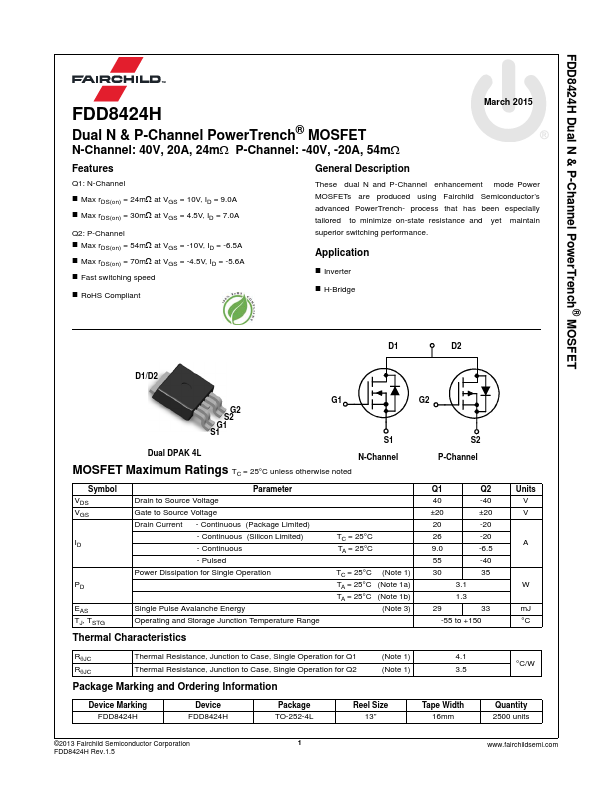
D1
D2
D1/D2
www.DataSheet4U.com
G1 G2 S2 G1 S1 S1 Dual DPAK 4L N-Channel
G2
S2 P-Channel
MOSFET Maximum Ratings TC = 25°C unless otherwise noted
Symbol VDS VGS Parameter Drain to Source
Voltage Gate to Source
Voltage Drain Current ID - Continuous (Package Limited) - Continuous (Silicon Limited) - Continuous - Pulsed Power Dissipation for Single Operation PD EAS TJ, TSTG Single Pulse Avalanche Energy Operating and Storage Junction Temperature Range TC = 25°C (Note 1) TA = 25°C (Note 1a) TA = 25°C (Note 1b) (Note 3) 29 TC = 25°C TA = 25°C Q1 40 ±20 20 26 9.0 55 30 3.1 1.3 33 mJ °C -55 to +150 Q2 -40 ±20 -20 -20 -6.5 -40 35 W A Units V V
Thermal Characteristics
RθJC RθJC Thermal Resistance, Junction to Case, Single Operation for Q1 Thermal Resistance, ...