FDC638APZ P-Channel 2.5V PowerTrench® Specified MOSFET
December 2006
FDC638APZ
P-Channel 2.5V PowerTrench® Specified ...
FDC638APZ P-Channel 2.5V PowerTrench® Specified
MOSFET
December 2006
FDC638APZ
P-Channel 2.5V PowerTrench® Specified
MOSFET
–20V, –4.5A, 43mΩ Features
Max rDS(on) = 43mΩ at VGS = –4.5V, ID = –4.5A Max rDS(on) = 68mΩ at VGS = –2.5V, ID = –3.8A Low gate charge (8nC typical). High performance trench technology for extremely low rDS(on). SuperSOTTM –6 package:small footprint (72% smaller than standard SO–8) low profile (1mm thick). RoHS Compliant
General Description
This P-Channel 2.5V specified
MOSFET is produced using Fairchild Semiconductor’s advanced PowerTrench® process that has been especially tailored to minimize the on-state resistance and yet maintain low gate charge for superior switching performance These devices are well suited for battery power applications:load switching and power management,battery charging circuits,and DC/DC conversion.
Application
DC - DC Conversion
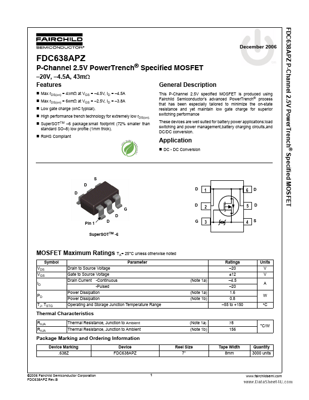
S D D
www.DataSheet4U.com
D
1 2
3 3
6
D
G D Pin 1 D
D
5
4
D
G
S
SuperSOTTM -6
MOSFET Maximum Ratings TA= 25°C unless otherwise noted
Symbol VDS VGS ID PD TJ, TSTG Parameter Drain to Source
Voltage Gate to Source
Voltage Drain Current -Continuous -Pulsed Power Dissipation Power Dissipation Operating and Storage Junction Temperature Range (Note 1a) (Note 1b) (Note 1a) Ratings –20 ±12 –4.5 –20 1.6 0.8 –55 to +150 Units V V A W °C
Thermal Characteristics
RθJA RθJA Thermal Resistance, Junction to Ambient Thermal Resistance, Junction to Ambient (Note 1a) (Note 1b) 78 156 °C/...