W-CDMA 1
www.datasheet4u.com
Customer Name System FMD Part Number Customer No.
Standard specification W-CDMA I (2G) Tx FAR-F6KA...
Description
www.datasheet4u.com
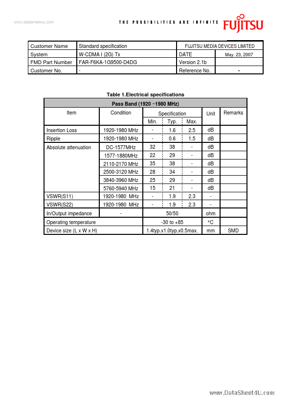
Customer Name System FMD Part Number Customer No.
Standard specification W-CDMA I (2G) Tx FAR-F6KA-1G9500-D4DG -
FUJITSU MEDIA DEVICES LIMITED
DATE Version 2.1b Reference No. May. 23, 2007
Table 1.Electrical specifications
Pass Band (1920 ~1980 MHz) Item Condition Min. Insertion Loss Ripple Absolute attenuation 1920-1980 MHz 1920-1980 MHz DC-1577MHz 1577-1880MHz 2110-2170 MHz 2500-3120 MHz 3840-3960 MHz 5760-5940 MHz VSWR(S11) VSWR(S22) In/Output impedance Operating temperature Device size (L x W x H) 1920-1980 MHz 1920-1980 MHz 32 22 35 28 25 15 Specification Typ. 1.6 0.6 38 29 38 34 29 21 1.9 1.9 50/50 -30 to +85 1.4typ.x1.0typ.x0.5max. Max. 2.5 1.5 2.3 2.3 dB dB dB dB dB dB dB dB ohm °C mm SMD Unit Remarks
www.datasheet4u.com
Customer Name System FMD Part Number Customer No.
Standard specification W-CDMA I (2G) Tx FAR-F6KA-1G9500-D4DG -
FUJITSU MEDIA DEVICES LIMITED
DATE Version 2.1b Reference No. May. 23, 2007
Dimensions
Device size: 1.4typ. x 1.0typ. x 0.5max.
Unit : mm
Pin Configuration
Pin No.
1 2 3 4 5
Symbol
IN GND GND OUT GND
Function
Unbalanced pin Ground Ground Unbalanced pin Ground
Evaluation Circuit
1 Unbalanced Input (50ohm) 2,3,5
4 Unbalanced Output (50ohm)
www.datasheet4u.com
Customer Name System FMD Part Number Customer No.
Standard specification W-CDMA I (2G) Tx FAR-F6KA-1G9500-D4DG -
FUJITSU MEDIA DEVICES LIMITED
DATE Version 2.1b Reference No. May. 23, 2007
Fig.1 Pass-band Characteristics
S11 S22
Fig.2 VSWR
www...
Similar Datasheet