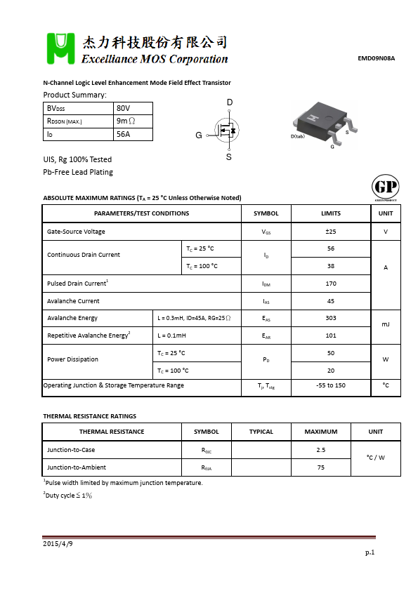
N‐Channel Logic Level Enhancement Mode Field Effect Transistor
Product Summary:
BVDSS
80V
D
RDSON (MAX.)
...
N‐Channel Logic Level Enhancement Mode Field Effect Transistor
Product Summary:
BVDSS
80V
D
RDSON (MAX.)
9mΩ
ID 56A G
UIS, Rg 100% Tested
S
Pb‐Free Lead Plating
ABSOLUTE MAXIMUM RATINGS (TA = 25 °C Unless Otherwise Noted)
PARAMETERS/TEST CONDITIONS
SYMBOL
Gate‐Source
Voltage
Continuous Drain Current Pulsed Drain Current1
TC = 25 °C TC = 100 °C
Avalanche Current
Avalanche Energy Repetitive Avalanche Energy2
L = 0.3mH, ID=45A, RG=25Ω
L = 0.1mH
Power Dissipation
TC = 25 °C TC = 100 °C
Operating Junction & Storage Temperature Range
THERMAL RESISTANCE RATINGS
THERMAL RESISTANCE
SYMBOL
VGS ID IDM IAS EAS EAR PD Tj, Tstg
TYPICAL
Junction‐to‐Case
RJC
Junction‐to‐Ambient
RJA
1Pulse width limited by maximum junction temperature. 2Duty cycle 1%
2...