N‐Channel Logic Level Enhancement Mode Field Effect Transistor
Product Summary:
BVDSS
100V
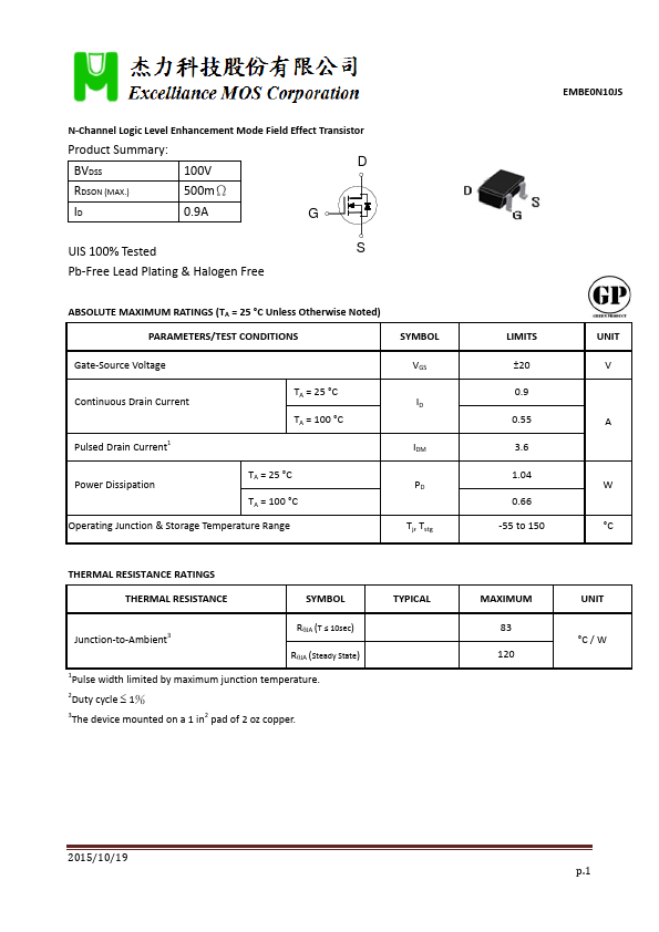
D
RDSON (MAX.)
...
N‐Channel Logic Level Enhancement Mode Field Effect Transistor
Product Summary:
BVDSS
100V
D
RDSON (MAX.)
500mΩ
ID 0.9A G
UIS 100% Tested
S
Pb‐Free Lead Plating & Halogen Free
ABSOLUTE MAXIMUM RATINGS (TA = 25 °C Unless Otherwise Noted)
PARAMETERS/TEST CONDITIONS
SYMBOL
Gate‐Source
Voltage
Continuous Drain Current Pulsed Drain Current1
TA = 25 °C TA = 100 °C
Power Dissipation
TA = 25 °C TA = 100 °C
Operating Junction & Storage Temperature Range
VGS ID IDM PD Tj, Tstg
EMBE0N10JS
LIMITS ±20 0.9 0.55 3.6 1.04 0.66
‐55 to 150
UNIT V
A
W °C
THERMAL RESISTANCE RATINGS THERMAL RESISTANCE
SYMBOL
Junction‐to‐Ambient3
RJA (T ≤ 10sec) RJA (Steady State)
1Pulse width limited by maximum junction temperature. 2Duty cycle 1% 3The device mounted on a 1 in2 pad o...