DS92LV010A
www.ti.com
SNLS007E – MAY 1998 – REVISED APRIL 2013
DS92LV010A Bus LVDS 3.3/5.0V Single Transceiver
Check ...
DS92LV010A
www.ti.com
SNLS007E – MAY 1998 – REVISED APRIL 2013
DS92LV010A Bus LVDS 3.3/5.0V Single Transceiver
Check for Samples: DS92LV010A
FEATURES
1
2 Bus LVDS Signaling (BLVDS) Designed for Double Termination Applications Balanced Output Impedance Lite Bus Loading 5pF Typical Glitch Free Power Up/Down (Driver Disabled) 3.3V or 5.0V Operation ±1V Common Mode Range ±100mV Receiver Sensitivity High Signaling Rate Capability (Above 100
Mbps) Low Power
CMOS Design Product Offered in 8 Lead SOIC Package Industrial Temperature Range Operation
DESCRIPTION
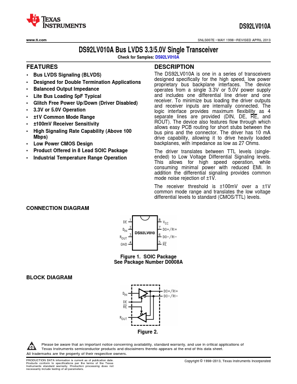
The DS92LV010A is one in a series of transceivers designed specifically for the high speed, low power proprietary bus backplane interfaces. The device operates from a single 3.3V or 5.0V power supply and includes one differential line driver and one receiver. To minimize bus loading the driver outputs and receiver inputs are internally connected. The logic interface provides maximum flexibility as 4 separate lines are provided (DIN, DE, RE, and ROUT). The device also features flow through which allows easy PCB routing for short stubs between the bus pins and the connector. The driver has 10 mA drive capability, allowing it to drive heavily loaded backplanes, with impedance as low as 27 Ohms.
The driver translates between TTL levels (singleended) to Low
Voltage Differential Signaling levels. This allows for high speed operation, while consuming minimal power with reduced EMI. In addition the differenti...